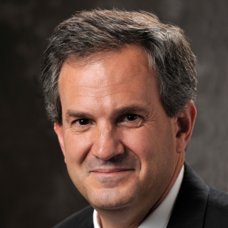
Craig L. Keast

Dr. Craig L. Keast is the associate head of the Advanced Technology Division and the director of operations for the Microelectronics Laboratory at MIT Lincoln Laboratory. The Advanced Technology Division performs research in high-performance imaging sensors, deeply scaled silicon microelectronics, solid-state lasers, optoelectronics, superconductive devices, and biological sensors.
Keast began his career at Lincoln Laboratory in 1981 as a semiconductor process technician in the Digital Integrated Circuits Group, where he helped fabricate some of the first wafer-scale integrated circuits. From 1988 to 1992, as a Kodak Fellow, he pursued his graduate studies at MIT, developing processes and circuits for analog machine vision applications. In 1992, Keast returned to Lincoln Laboratory as a technical staff member in the Submicrometer Technology Group, working on deeply scaled device development using advanced optical lithography techniques. In 1994, he became the Director of Operations for the Microelectronics Laboratory, Lincoln Laboratory's semiconductor fabrication facility; in 1996, he became the Leader of the Advanced Silicon Technology Group. In addition to providing oversight for the Microelectronics Laboratory, this group's research activities include fully depleted silicon-on-insulator CMOS process development for ultralow-power and extreme environment operation; three-dimensional circuit integration technology for high-performance imaging applications; RF, optical, and microfluidic microelectromechanical systems; and advanced focal plane readout integrated-circuit design.
Keast holds a BA degree from Hamilton College and SM, EE, and PhD degrees in electrical engineering and computer science from MIT. He has authored or coauthored numerous papers in the advanced electronics technology area.