Facilities
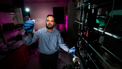
Biophotonic, Electric, Acoustic, and Magnetic Measurement Laboratory
MIT Lincoln Laboratory
The BEAMM Lab allows staff to study biological tissue and its interactions with energy and technology.
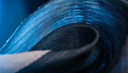
Defense Fabric Discovery Center
MIT Lincoln Laboratory
The DFDC houses technology to develop advanced fibers and fabrics for defense applications.
Electronic-Photonic Integration Facility
MIT Lincoln Laboratory
The state-of-the-art facility supports the development of optoelectronic components, photonic integrated circuits, CMOS electronic integrated circuits, and hybrid electronic-photonic integration techniques.
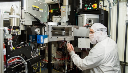
Microelectronics Laboratory
MIT Lincoln Laboratory
The Microelectronics Laboratory is a state-of-the-art semiconductor research and fabrication facility that supports the design, fabrication, and packaging of novel devices.
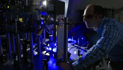
Quantum Computing Laboratory
MIT Lincoln Laboratory
We are studying methods to use trapped ions and Josephson junction–based superconducting circuits for large-scale quantum information processing.
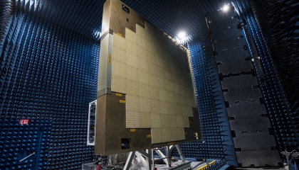
RF Systems Test Facility
MIT Lincoln Laboratory
The facility enables us to fabricate, integrate, and test in anechoic chambers RF systems to ensure they will work well in the field.