Defensive Wire Routing for Untrusted Integrated Circuit Fabrication
MIT Lincoln Laboratory developed defensive wire routing technology to deter an outsourced foundry from maliciously tampering with or modifying security-critical components of a digital circuit design. By rendering hardware modifications readily detectable, this method reduces the risk of a compromise to a circuit design and improves cybersecurity and mission assurance even when components are fabricated at untrusted facilities.
Motivation
Economic forces are driving a global consolidation of integrated circuit (IC) fabrication facilities (i.e., foundries) overseas. While microprocessors are achieving increased performance with smaller transistors, system developers find that access to trusted high-performance foundries is decreasing, thereby disadvantaging systems, such as U.S. government ones, that require high degrees of trust. One concern with untrusted fabrication is malicious modification or tamper, whereby a trusted design is modified by a fabricator to insert a “hardware Trojan” or “backdoor” that can compromise downstream system security. Therefore, there is demand for design-time methods that deter and/or prevent malicious modification so that developers can make trusted use of ICs fabricated by untrusted foundries.
Concept
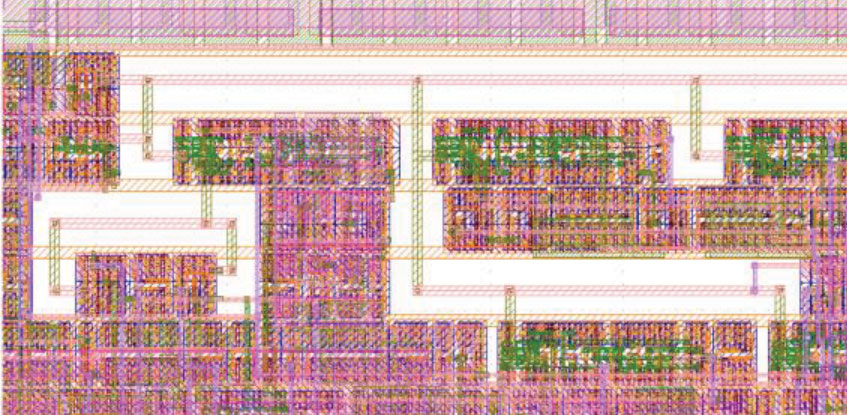
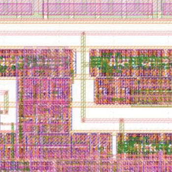
The routing of wires within ICs is a complex process in which conductive metallization is planned and deconflicted across multiple planer layers of silicon to route and interconnect signals between logic devices such as transistors. The Defensive Wire Routing technology employs two complementary techniques to deter tampering with the wiring. Both techniques could be integrated as semiautomated features into electronic design automation tools commonly used for the design and layout of digital integrated circuits.
- “Keep-out zones” are built around identified, security-critical signals, creating an inspectable window, or “porthole,” that allows designers to spot a “rogue” wire-post on the chip that indicates a suspicious, or malicious, modification.
- Displacement of guard wires that protect designer-identified, security-critical wires from modification indicates tampering. Guard wires are designated as “natural” (existing functional interconnects in the design) or “synthetic” (new interconnects that must be displaced to route a rogue wire).
Benefits
- Enables post-fabrication verification to ensure that a defensive solution was truly effective
- Does not require destructive inspection (unlike a traditional scanning electron microscope inspection)
- Can be applied to every chip because it adds very little extra circuitry
- Minimizes overhead costs because the technique can be focused on security-critical components
Additional Resources
U.S. Patent 10,839,109
More Information
T. Trippel, K.G. Shin, K. Bush, and M. Hicks, “T-TER: Defeating A2 Trojans with Targeted Tamper-Evident Routing,” preprint, 27 Oct. 2020.