Extremely Large-Area Integrated Circuit: New Era for Chiplet Integration
A novel, heterogeneous chip tiling enables the development of highly secured, extremely large-area integrated circuits (ELAICs) with hundreds of closely spaced small chips (called chiplets) fabricated via a lithographic process (5-, 7-, or 10-nanometer). These ELAICs address the increasing size and performance demands made on microelectronics used in mobile devices, complex sensing systems, high-performance computing, and the automotive, healthcare, and aerospace industries.
Much of the world is experiencing a digital transformation—a fundamental shift to digital technologies for managing work and business processes. The demands on the computing and connectivity enabling applications for this transformation are driving the microelectronics industry toward cost-driven, multifunctional, miniaturized technology with increased performance and decreased power consumption.
The basic concept of Lincoln Laboratory's ELAIC approach is to assemble small specialized chips, called chiplets, into a single-chip-like monolithic integrated circuit. The ELAIC interconnected structure extends packaging performance beyond the limits imposed by traditional wafer-level packaging. Multiple heterogeneous chiplets are interconnected within layers that redistribute (reroute) the electrical inputs and outputs to enable high-bandwidth, low-latency chiplet-to-chiplet communication. This architecture relies on fine lines and spaces to achieve high-density circuits. The ELAIC structure of very thin layers not only allows circuit density but also improves package stability and reliability by minimizing thermal variations caused by the flip-chip-integrated chiplets.
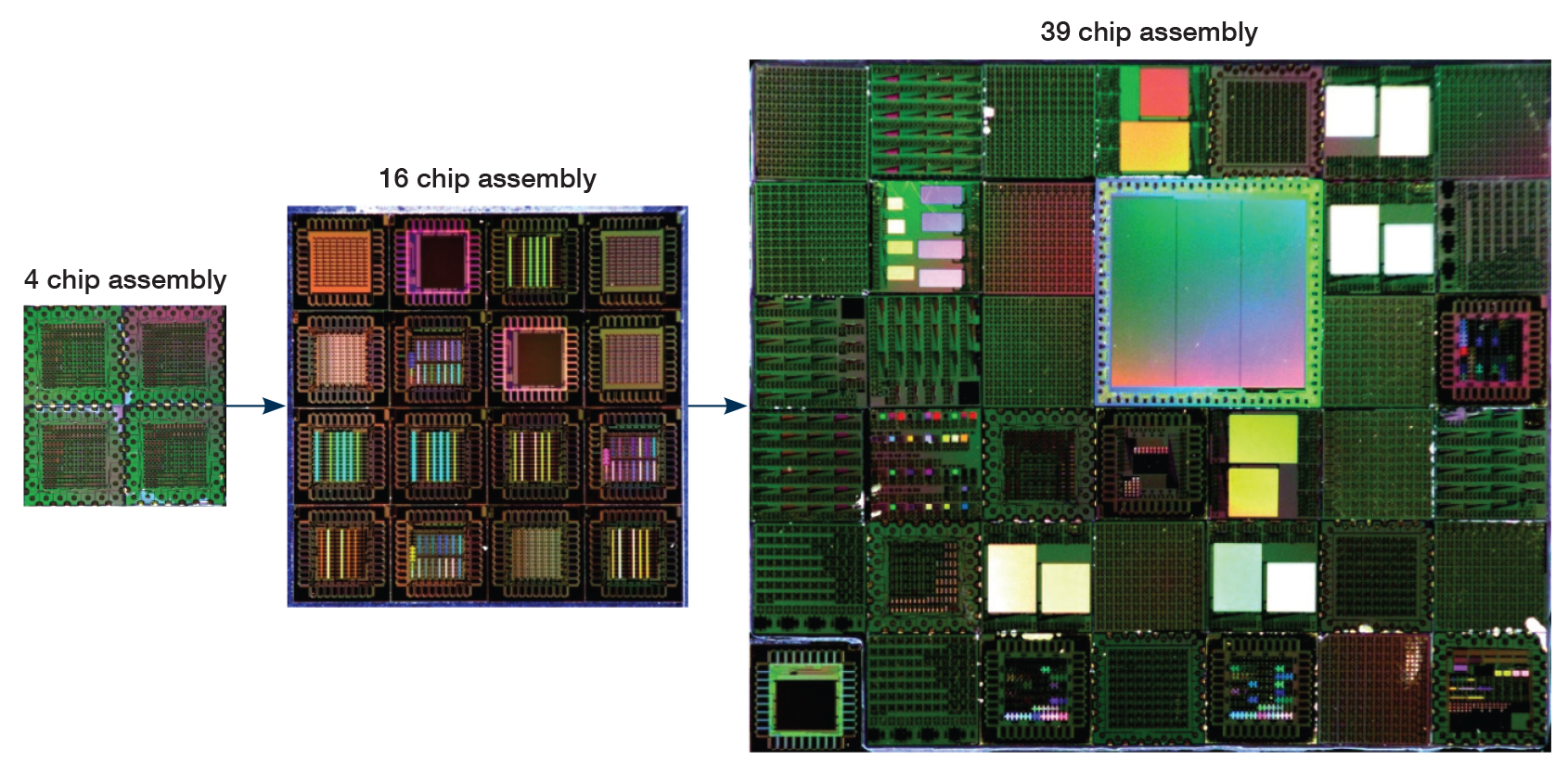
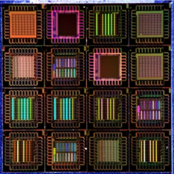
This figure illustrates the ELAIC concept in which known reliable chips (fabricated from both the same or different processes) are combined to make a device that performs like a single chip. The ELAIC fabrication process can be scaled for various-sized chip assemblies. The image shows assemblies ranging from 4 to 16 to 39 chips. The process has the potential to scale to much larger monolithic chip-like assemblies.
For modern applications that rely heavily on artificial intelligence, machine learning, and embedded computing, power consumption comes from moving data between chips in a system rather than from actual computing. The ELAIC approach reduces data movement constraints by integrating multiple chiplets with minimum chip-to-chip spacing (e.g., 5- to 20-micrometer separation between chips).
By integrating multiple chiplets into one large-area chip (2D array), the ELAIC approach can help solve two challenges to the microelectronics industry: expanding the yield of chip manufacture and reducing both cost and time to develop systems.
Benefits
- The ELAIC approach allows trusted and commercial foundry chips to be combined to create highly secured systems in which the commercial chips provide circuit density and performance, and the trusted foundry chips add system security
- The assembly of an ELAIC from multiple known chips—i.e., proven reliable and/or fabricated by trusted foundries—reduces R&D costs in developing new heterogeneous systems
- The ELAIC structure with 5- to 20-micrometer (µm) chip-to-chip spacing creates short (50 to 500 µm) communication links for a high-efficiency power-delivery network
- An ELAIC chip has a silicon content of about 99%, allowing highly stable and inexpensive fabrication of a multi-die system-on-chip with chip-like wiring density
Potential Use Cases
- High-performance computing and artificial intelligence
- Mobile devices
- Sensors
Additional Resources
R. Das et al., "Extremely Large Area (88 mm × 88 mm) Superconducting Integrated Circuit (ELASIC)," Science Reports, 13, article #11796, 2023..