
MIT engineers “grow” atomically thin transistors on top of computer chips
Emerging AI applications, like chatbots that generate natural human language, demand denser, more powerful computer chips. But semiconductor chips are traditionally made with bulk materials, which are boxy 3D structures, so stacking multiple layers of transistors to create denser integrations is very difficult.
However, semiconductor transistors made from ultrathin 2D materials, each only about three atoms in thickness, could be stacked up to create more powerful chips. To this end, MIT researchers have now demonstrated a novel technology that can effectively and efficiently “grow” layers of 2D transition metal dichalcogenide (TMD) materials directly on top of a fully fabricated silicon chip to enable denser integrations.
Growing 2D materials directly onto a silicon CMOS wafer has posed a major challenge because the process usually requires temperatures of about 600 degrees Celsius, while silicon transistors and circuits could break down when heated above 400 degrees. Now, the interdisciplinary team of MIT researchers has developed a low-temperature growth process that does not damage the chip. The technology allows 2D semiconductor transistors to be directly integrated on top of standard silicon circuits.
In the past, researchers have grown 2D materials elsewhere and then transferred them onto a chip or a wafer. This often causes imperfections that hamper the performance of the final devices and circuits. Also, transferring the material smoothly becomes extremely difficult at wafer-scale. By contrast, this new process grows a smooth, highly uniform layer across an entire 8-inch wafer.
The new technology is also able to significantly reduce the time it takes to grow these materials. While previous approaches required more than a day to grow a single layer of 2D materials, the new approach can grow a uniform layer of TMD material in less than an hour over entire 8-inch wafers.
Due to its rapid speed and high uniformity, the new technology enabled the researchers to successfully integrate a 2D material layer onto much larger surfaces than has been previously demonstrated. This makes their method better-suited for use in commercial applications, where wafers that are 8 inches or larger are key.
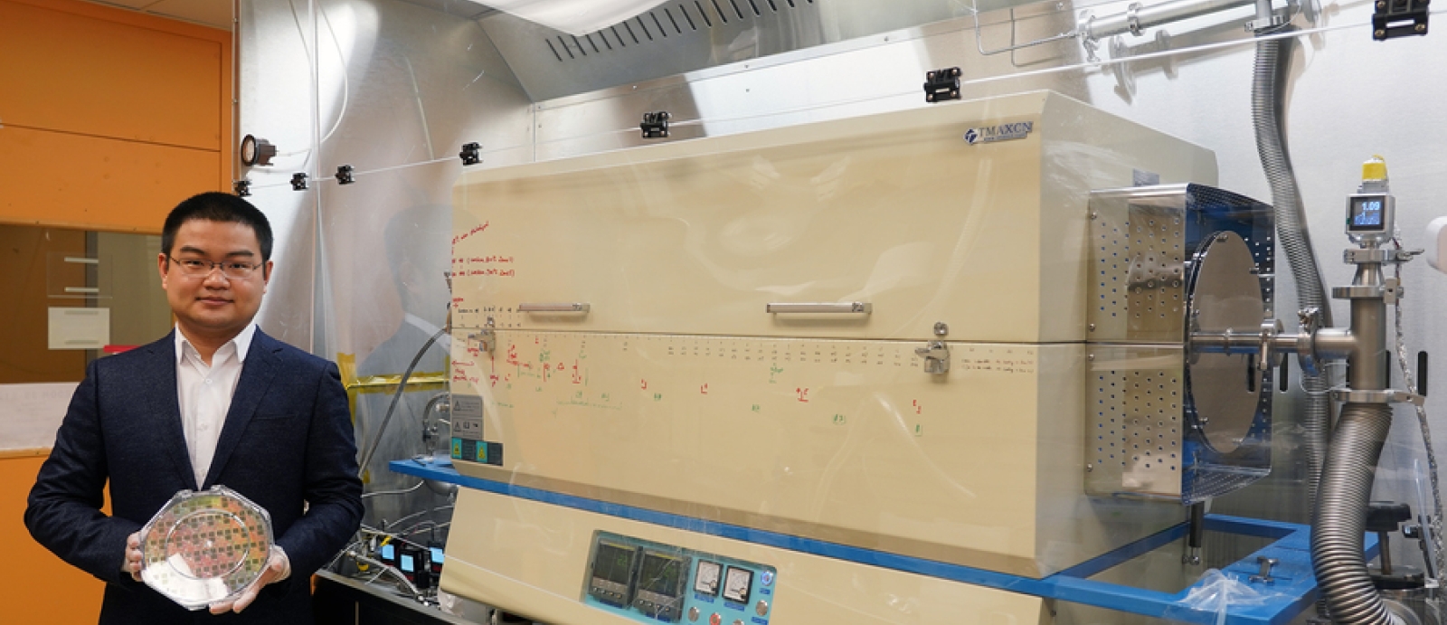
“Using 2D materials is a powerful way to increase the density of an integrated circuit. What we are doing is like constructing a multistory building. If you have only one floor, which is the conventional case, it won’t hold many people. But with more floors, the building will hold more people that can enable amazing new things. Thanks to the heterogenous integration we are working on, we have silicon as the first floor and then we can have many floors of 2D materials directly integrated on top,” says Jiadi Zhu, an electrical engineering and computer science graduate student and co-lead author of a paper on this new technique.
Zhu wrote the paper with co-lead-author Ji-Hoon Park, an MIT postdoc; corresponding authors Jing Kong, professor of electrical engineering and computer science (EECS) and a member of the Research Laboratory for Electronics; and Tomás Palacios, professor of EECS and director of the Microsystems Technology Laboratories (MTL); as well as others at MIT, MIT Lincoln Laboratory, Oak Ridge National Laboratory, and Ericsson Research. The paper appears today in Nature Nanotechnology.