
Active Wafer-Scale Reconfigurable Logic Fabric for AI and High-Performance Embedded Computing
High-performance computing and AI workloads place unprecedented demands on on-chip communication bandwidth and latency, driving a shift toward tightly integrated multichip assemblies. Traditional printed circuit board (PCB) and interposer-based packaging architectures struggle to keep pace with the data rates required by deep learning inference and signal processing workloads, which require chip-to-chip interconnects approaching the density and speed of on-chip wiring. As the sizes of integrated circuit (IC) features shrink and heterogeneous accelerators become commonplace, the gap between die-to-die and intra-die communication grows, creating bottlenecks that throttle system-level throughput and efficiency.
Conventional approaches rely on discrete chip packaging with relatively coarse-pitch solder balls or wire bonds, resulting in long interconnect paths, high parasitic capacitance, and limited routing density. Large reticle stitching techniques for monolithic dies introduce manufacturing complexity and low yields, making wafer-scale integration impractical. Existing interposer solutions provide modest improvements but still suffer from thermal hotspots caused by uneven power distribution and limited cooling pathways. Moreover, the lack of fine-grained defect mitigation and reconfigurability means that single-point failures can render entire modules unusable, driving up costs and reducing system reliability.
Technology Description
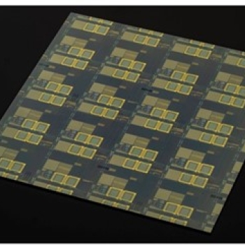
An active–passive wafer-scale logic fabric integrates hundreds of bare-die chips into a single, monolithic device by combining a solder-compatible under-bump metal (UBM) layer with μ-bump flip-chip bonding to heterogeneous ICs and a base interposer or PCB substrate. Multiple passive routing layers, implemented with transistor-based switches or routing chiplets, can be masklessly reconfigured to bypass defects discovered during wafer-scale testing. Through-silicon vias link the fabric's opposing surfaces, while hierarchical interconnect pitches use distinct solder or metal alloys to optimize signal integrity at each integration level. Integrated cooling structures — such as micro-channels and micro-jets—are embedded directly into the wafer, and the fabrication flow merges EX4 deep-ultraviolet (DUV) lithography for active device layers with large-field i-line reticles and stitching for interconnects up to 88 mm², rounded out by laser direct-write (LDW) or contact lithography to complete full-die circuitization.
This approach is differentiated by its ability to provide chip-like wiring density across a heterogeneous multichip assembly, delivering higher bandwidth and lower latency than achievable by traditional packaging. Maskless reconfiguration of passive routing layers enables yield enhancement and defect tolerance at wafer scale. The use of multiple melt-temperature interconnects permits hierarchical assembly steps without reflow interference, while embedded cooling ensures thermal management at high power densities. Unifying active device fabrication, reconfigurable routing, heterogeneous chiplet integration, and advanced thermal solutions in a single wafer platform creates a scalable, fault-tolerant substrate ideally suited for AI and high-performance embedded computing.
Benefits
- Monolithic-scale performance by seamlessly tiling known-good chips into a single wafer-scale device
- Ultra-high bandwidth and low-latency "chip-like" interconnects between heterogeneous chiplets
- Maskless, transistor-based reconfiguration of passive routing layers to bypass defects and boost yield
- Hierarchical interconnect pitches and multi-melt-temperature solder alloys for optimized 2D/3D integration
- Integrated micro-channel and micro-jet cooling structures for efficient thermal management
- Reduced connectivity loss and power consumption compared to conventional board-level packaging
- Flexible multilevel lithography (EX4 DUV, i-line stitching, LDW) enabling full-wafer circuitization and cost-effective manufacturing
Potential Use Cases
- Neural network training accelerators
- AI inference servers
- Data-center reconfigurable field-programmable fate arrays
- Real-time image processors
- Autonomous vehicle computers