
Advancing Computing with Novel Bumpless Chiplet Integration
Technology Description
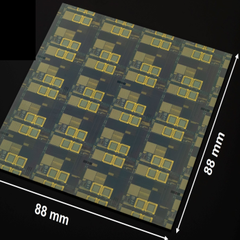
Researchers at Lincoln Laboratory have developed an innovative approach to fabricating 3D integrated circuits with lower latency and higher power efficiency than achieved by other 3D integrated circuits. The technique uses an AI decision-tree-optimized fabric, combined with a digital layer heterogeneously integrated to hundreds of closely spaced bumpless chiplets, to enable a fully functional, low-cost, high-yield system.
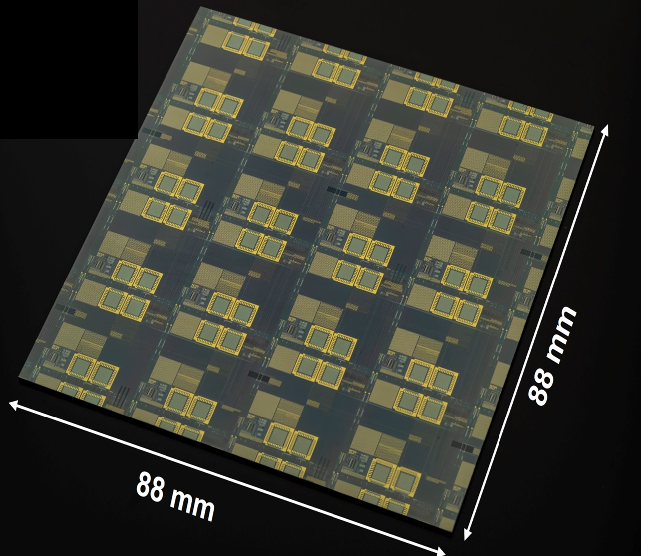
This bumpless chiplet integration allows interconnection of the massive number of electrical components (e.g., transistors, resistors, capacitors, diodes) necessary for powering today’s and the future’s AI neural networks, mobile devices, servers, and high-performance classical and quantum computing.
Background
Modern computing demands for high-density semiconductor integrated circuits have led to significant changes in chip design and manufacturing. Computer designers are exploring heterogeneous 3D stacked assemblies of specialized chips (called chiplets) to provide integrated circuits capable of powering our data-intensive world. To create compact stacks, designers are using a microbump fabrication technique in which tiny bumps of conductive material provide the electrical connections between the layers of the integrated circuit. This technique can enable dense interconnections that speed up signal processing and lower energy output. Yet, the growing need for more computing capability and further miniaturization means that the tight spacing of the microbump connections (input/output [I/O] pitch) is still not tiny enough to accommodate the massively interconnected components needed for the next generation of powerful microcomputers.
Innovation: Bumpless Integration
Lincoln Laboratory researchers have developed a novel technique that eliminates microbumps, allowing the integration of massive numbers of chiplets into a system that performs like a single chip. And, by enabling the co-location of memory and processor, the bumpless approach helps reduce latency and energy costs for real-time data processing.
The key to this technique is the use of a bumpless fabric that allows the electrical bonding of the layers of the chiplet stack. The researchers employed an AI-driven decision-tree algorithm to optimize the design of lithographically produced fabric that supplies the necessary configuration for the interconnections.
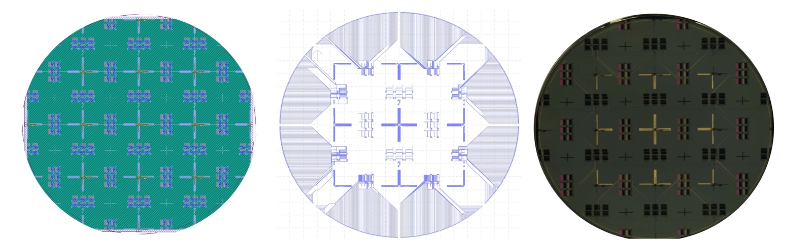
The decision-tree optimization begins with individual I-line lithographic circuits and interconnection/stitching schemes (stitched reticle graphical layer) (a); a digital layer (b) is then designed to interconnect the stitched reticle layer to the wafer (c) with a maskless digital layer.
Bumpless AI-optimized-fabric integration offers not only improved computing capability but also manufacturing advantages. Approved chiplets from any foundry can be integrated directly to the AI-optimized fabric. Process costs are also reduced because bumpless technology does not require post-chiplet processing as does the microbump technique. A proposed method for promptly detecting defects in a full-wafer circuit utilizes AI image recognition, potentially facilitating increased chip production.
Benefits
- Achieves very narrow inter-chip spacing with tiny interconnections between pins (i.e., I/O pitch) to enable high bandwidth, fast signal transmission with low link energy
- Lowers manufacturing costs and increases chiplet yield by using known good chiplets from any foundry process nodes, integrating them directly to the AI-optimized fabric, and eliminating post-chiplet processing
- Reduces the temperature difference between the chiplets within a 3D stack to allow for improved efficiency and speed in accessing memory and other functionalities
- Allows memory to be very close to the processor to reduce latency for real-time processing and reduce the energy cost of data movement
Additional Resources
U.S. Patent Application 18/883,881
R. N. Das et al., “AI-Based Decision-Tree Concept to Fabricate Active Waferscale Fabric for Heterogeneous Chiplet Integration,” 2025 IEEE 75th Electronic Components and Technology Conference, 27−30 May 2025.
2025 R&D 100 Award Winner