
Enabling Rapid Development of Advanced Imaging Sensors
MIT Lincoln Laboratory has pioneered fabrication technology that supports the rapid development of advanced imaging sensors. Innovative engineered substrates allow most steps of back-illumination to be built directly into a wafer containing arrays of light-sensing detectors, i.e., photodetectors. A rapid prototyping process mates single dies cut from the detector wafer to individual readout integrated circuits (ROICs). Because costly, time-intensive, and precise coupling of full detector wafers to full ROIC wafers is eliminated, this technology promotes the invention of highly unique imaging sensors for specialized scientific research and other uses.
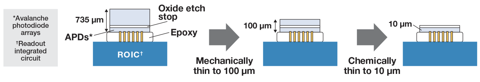
In the chip-level thinning process, the silicon detector layer is bump-bonded to the readout integrated circuit (ROIC) and underfilled with epoxy that provides mechanical support after the device layer is thinned down to 10 µm. A mechanical process then a chemical etching process remove the bulk of the opaque substrate.
Background
Modern imaging sensors rely on the integration of photodetectors, which sense light and convert it into an electrical signal, with readout circuitry that digitizes the photodetector signal. A common technique bonds separate semiconductor wafers featuring silicon- or germanium-based detectors together with wafers containing the readout circuitry. This approach requires a costly full-wafer foundry run to build the readout circuits, potentially extending to more than a million dollars, and has other drawbacks:
• Bonding a pair of 8- or 12-inch-diameter wafers places stringent requirements on wafer planarity and surface smoothness.
• The traditional, distinct, heavily doped backside contact layer, needed for good performance, requires high process temperatures that risk damaging detectors, circuits, or interconnects.
• Wafer-to-wafer alignment requires detector arrays and pixel circuit arrays to be co-designed across the entire wafer area, precluding the use of known good detector and circuitry dies.
Innovative Solution
Our novel process begins with the fabrication of a custom, engineered-substrate wafer with a built-in backside electrical contact layer and buried oxide layer to define the active region of the detector. This wafer is diced into individual imager dies, which are then bump-bonded to individual readout circuitry dies. The necessary removal of the detector array’s opaque substrate material is done by using the engineered substate’s buried SiO2 layer as a built-in etch-stop.
The process enables a straightforward back-illumination process on small batches of detectors, lowers sensor noise, and allows uniform thinning of the detector layer down to a thickness of 1 µm or below for individual chips. Such thinning allows developers to stack multiple layers into 3D structures packing many components into miniaturized devices with low power requirements.
This invention has enabled the rapid, cost-effective development of new imaging sensors that would have taken years via a traditional process. An engineered substrate could be used as part of a full-wafer 3D integration process, enabling a well-vetted design to be efficiently transferred into large-scale production fabrication. Researchers have begun investigations into extending the engineered-substrate technology from silicon to other material systems.
Potential Use Cases
- Bump-bonding of detector die to circuit die eliminates (1) wafer planarity requirements and (2) iterations of dielectric deposition and chemical-mechanical polishing required of full-wafer bonding
- Engineered substrates enable uniform ultrathin (1 µm) detectors for fast photo-response
- Readout integrated circuits can be fabricated in multi-customer foundry runs
- Die-to-die integration can save millions of dollars because a dedicated full-wafer fabrication run is not needed
- Simplicity and cost-effectiveness of the process encourage development of new sensor designs and devices because less risk is involved in experimentation
Additional Resources
Patents pending, WO2020205045 and US18/155,876
K. Ryu et al., “Geiger-Mode Avalanche Photodiode Arrays Fabricated on SOI Engineered Substrates,” Proceedings of SPIE, 12089, Advanced Photon Counting Techniques XVI, 30 May 2022.
2024 R&D 100 Award Winner