
Innovative Cryomicroscope: Enabling Development of Next-Generation Computing
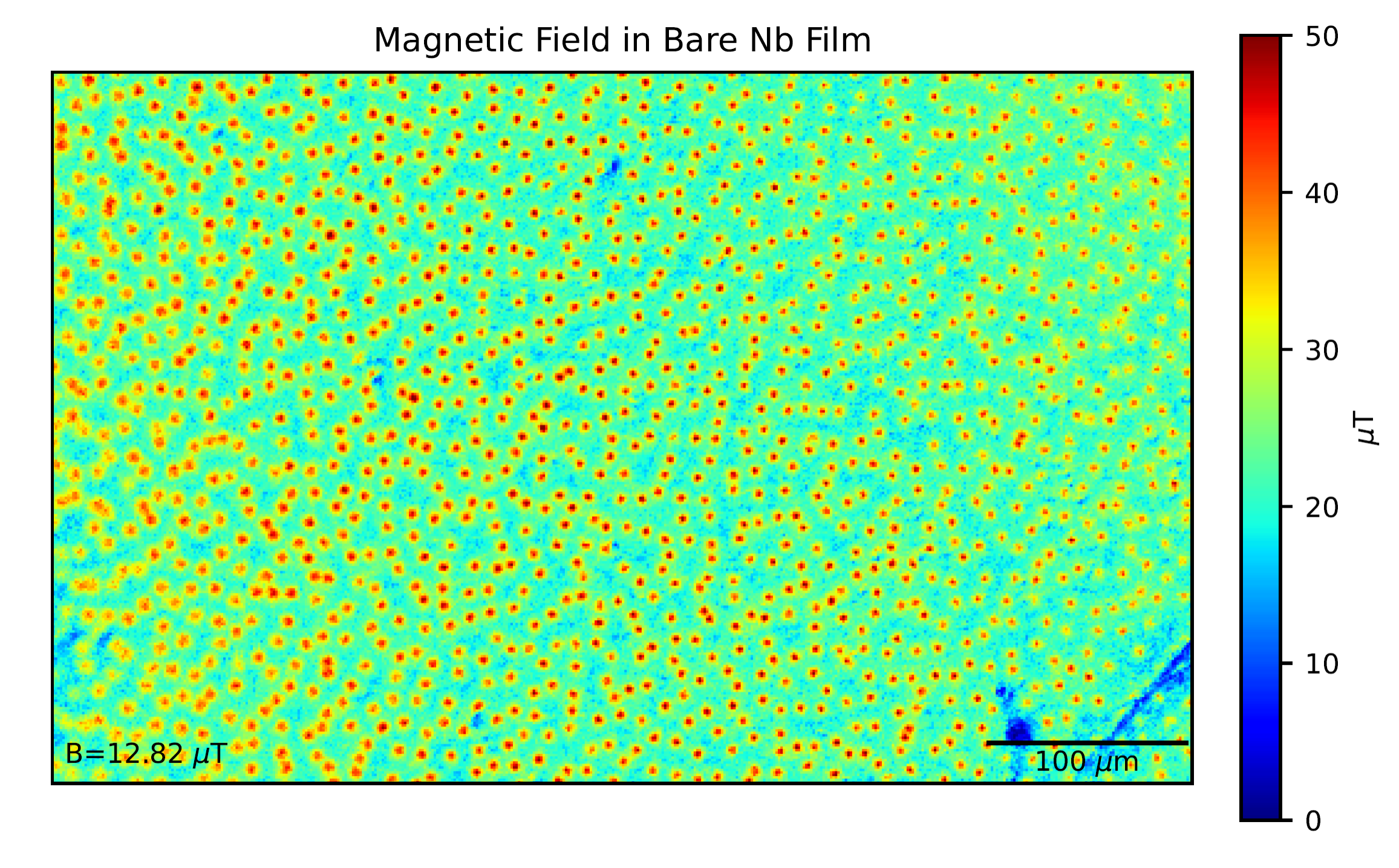
Researchers at Lincoln Laboratory have leveraged nitrogen-vacancy (NV) diamond capabilities to design a magnetic field imaging (MFI) device to support the development of advanced high-performance computers that utilize superconducting electronics. This cryomicroscope provides rapid, high-resolution MFI at the extremely low (i.e., cryogenic) temperatures needed to maintain cooling of the superconducting electronics. With this tool, developers of superconducting computing can visualize, analyze, and address the formation of quantized vortices (eddies of trapped magnetic flux) that are inherent in supercooled magnetic fields but interfere with the function of critical circuit components.
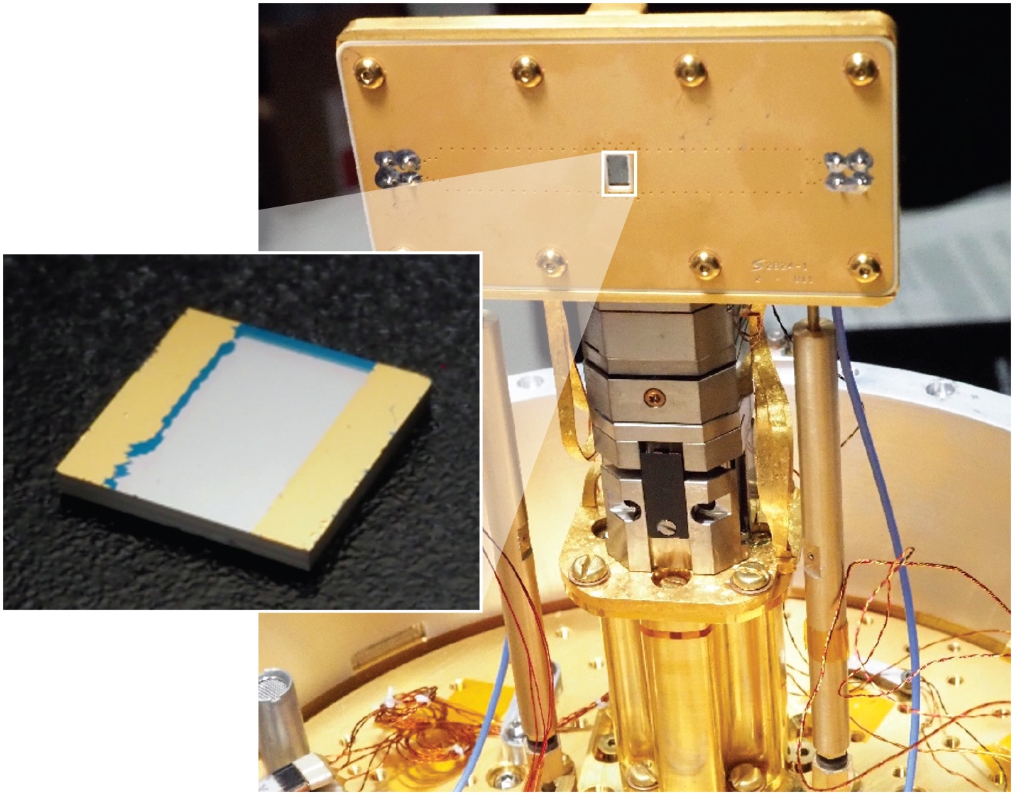
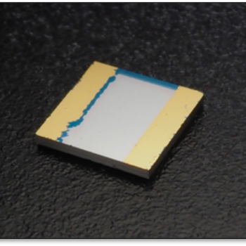
Inside the cryomicroscope’s optical cryostat sits a lab-grown diamond sample with a thin layer of magnetically sensitive nitrogen-vacancy (NV) centers (inset). Illuminating the NV layer with laser light and imaging the fluorescence light onto a camera enables visualization of the magnetic field distribution of a nearby superconducting device under test.
Motivation
Computing that employs superconducting electronics (SCE) offers speed and power efficiency dramatically higher than achievable by traditional semiconductor-based computers. These advantages are increasingly important to today’s data centers and applications that demand significant power capacity and exceptional computational performance.
Materials used in SCE—e.g., niobium and niobium nitride—operate at very low temperatures that require information to be encoded by using the smallest quantized units of magnetic flux governed by quantum mechanics. When a superconductor is cooled to its critical temperature in a magnetic field, magnetic flux can become trapped as quantized vortices that disrupt circuit operation. Discovering and understanding the behavior of these vortices has inhibited strategies to mitigate their effects and slowed the advance of SCE computing.
Innovation
Our widefield NV-diamond cryomicroscope is designed to identify vortex evolution and support development of mitigation strategies. It consists of a lab-grown diamond sample with NV centers placed on top of a superconducting circuit surface. The NVs are illuminated with green laser light, and a resonant microwave field is applied to interrogate the NVs. The NV layer is treated with a reflective coating to prevent light from reaching the SCE circuits, and the back of the diamond has an anti-reflection coating to prevent excess laser heating. The fluorescence light is then imaged with an optical microscope that generates camera images of the magnetic field in every pixel. This approach enables high-sensitivity MFI across a millimeter-scale field of view with micron-scale spatial resolution and a wide range of operating conditions.
Potential
The quantum diamond magnetic cryomicroscope’s approach could inform new SCE designs, mitigating the flux-trapping problem and enabling integration of SCE into computing systems. The technology may also be applied more broadly to enable diagnostics of active SCE devices, novel 2D magnetic materials, and even superconducting qubit circuits.
Benefits
- Fast-turnaround (minutes vs hours) MFI allows hundreds of measurements of superconducting devices and materials to enable comprehensive analysis of vortices
- Widefield scanning yields both spatial and temporal views of vortex evolution
- With almost no moving parts or fragile components, the cryomicroscope has worked for hundreds of hours with zero failures or breakages
- Operation of the system is straightforward enough that users need no elaborate training
Additional Resources
R.T Kapur, P. Kehayias, et al., “Flux Trapping Characterization for Superconducting Electronics Using a Cryogenic Widefield NV-Diamond Microscope,” arvix: Condensed Matter, Superconductivity, June 2, 2025.,” arvix: Condensed Matter, Superconductivity, June 2, 2025.
2025 R&D 100 Award Winner