
Government-Directed Technology Transfer of Photonic Multi-Chip Module (P-MCM) Platform
Overview
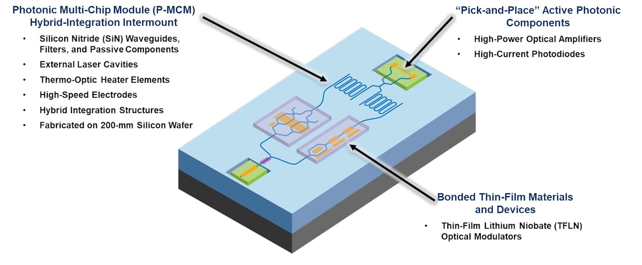
Through investment from the U.S. Government, MIT Lincoln Laboratory (MIT LL) has established a photonic multi-chip module (P-MCM) platform operating at optical wavelengths near 1550 nm (i.e., optical telecommunications C-band), which integrates silicon nitride (SiN) passive photonic components (e.g., waveguides, spitters/combiners, mode converters, optical filters), wideband thin-film lithium niobate (TFLN) electro-optic modulators, high-power low-noise external-cavity lasers (ECLs) incorporating on-chip InGaAsP/InP quantum-well semiconductor optical amplifier (SOA) gain media, and InGaAs-based high-current waveguide photodiodes on a common wafer-scale substrate. This investment has resulted in a novel hybrid integrated photonic platform containing components having state-of-the-art performance. Potential applications of the platform include microwave photonics, free-space lasercom, lidar and remote sensing, and atom-based quantum sensing and computing.
Figure 1 shows a schematic of the generic P-MCM architecture. Silicon-nitride (SiN) waveguide-based passive components and thermo-optic phase shifters are fabricated on silicon (Si) substrates using conventional silicon-fabrication tools to form the “intermount”, which provides photonic and electronic routing, photonic functionality such as filtering and phase control, and mechanical support. TFLN is integrated into the intermount to realize high-bandwidth modulators via surface bonding at the wafer scale. The active compound-semiconductor (III-V) components (e.g., SOAs, photodetectors) are grown and fabricated on native indium phosphide (InP) substrates, singulated, and flip-chip bonded into prepared trenches in the intermount. At the present time, photonic component and circuit design, intermount fabrication, TFLN bonding and processing, III-V component fabrication, and hybrid flip-chip integration are performed onsite at MIT LL using vertically integrated resources.
The U.S. Government has directed MIT LL to assess options for establishing a capability within U.S. industry to fabricate and supply photonic components and photonic integrated circuits (PICs) having key attributes comparable to or exceeding that of the P-MCM platform. It is anticipated that the resulting PIC fabrication and supply capability, including packaging and testing, will be offered in a way that assures the quality and timeliness of fabrication and assembly, protects the Government’s intellectual property (IP) and critical applications of the technology, and meets relevant export-control restrictions. The purpose of this request for information (RFI) is to solicit information from potential offerors of the photonic components and PIC platform to educate the Government on options to realize this capability within U.S. industry. The intent is to obtain a general understanding of existing resources and prior experience, proposed plans for how the capability would be established, and rough-order-of-magnitude (ROM) estimates of cost and schedule. This RFI should NOT be considered a call-for-proposals in a formal source-selection process.
We note that proposed plans to establish a complete end-to-end PIC/component foundry capability or to provide only portions of the fabrication and supply capabilities are both of interest. For instance, some offerors might only have the ability or interest to offer a portion of the fabrication process needed to create full components and/or PICs (e.g., fabrication of the silicon-based intermount, fabrication of the III-V lasers and/or photodetectors, hybrid integration of the intermount and the III-V-based components). Proposed plans to offer a fabless PIC integrator capability, in which the integrator coordinates U.S.-based fab resources to develop and offer the full PIC, are also welcome.
While the Government plans to make all of the MIT LL P-MCM platform IP available as part of the tech-transfer process, it is anticipated that some potential offerors will have existing fabrication processes for related photonic devices and processes that could be leveraged and/or combined with the P-MCM platform IP to create a PIC platform that meets the required performance specifications. The Government is interested in learning about these existing capabilities and IP that may be available. We note that proposals to develop new processes, components, or PIC platforms other than those associated with the P-MCM platform described in the full RFI document, and which have not been previously demonstrated by the responder, are outside the scope of this RFI.
Responders to the RFI are expected to provide the following elements of their plans:
- Technical approach
- Logistical plan
- ROM estimated development and offering costs
- ROM estimated development and cycle timelines
- Technology offering plan
- Technology protection plan
Instructions for Responders
Responders to this RFI will be limited to U.S.-based organizations capable of demonstrating that they are able to receive and generate controlled unclassified information (CUI) with export-control restrictions. To request a copy of the full CUI RFI document including the P-MCM performance specifications, responders should fill out the form below to obtain instructions on how to document their ability to receive the CUI RFI.