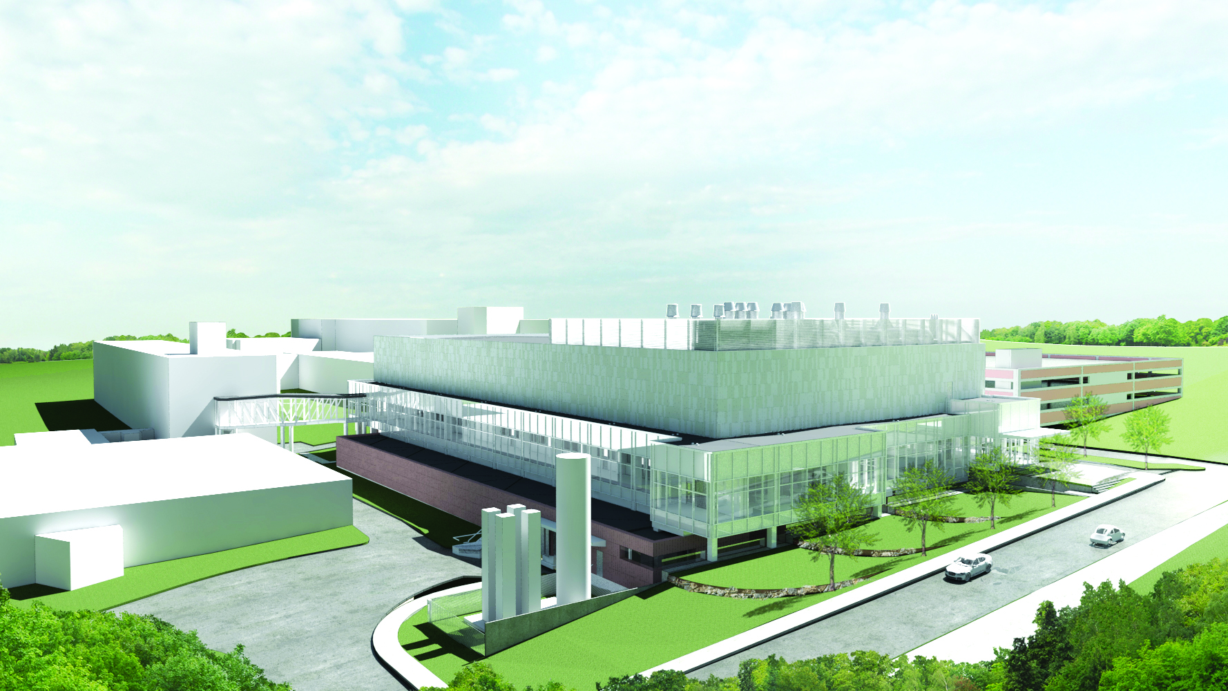
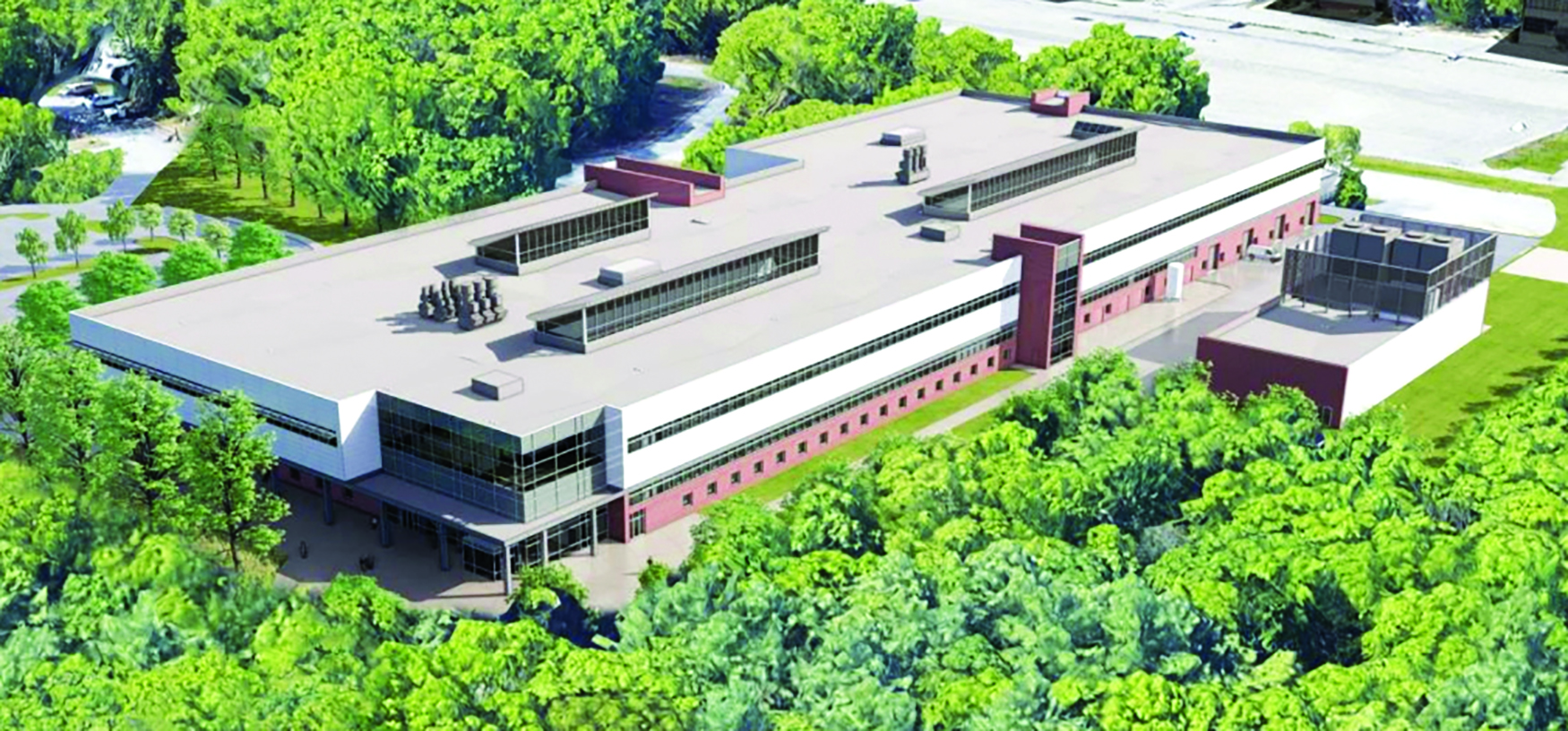
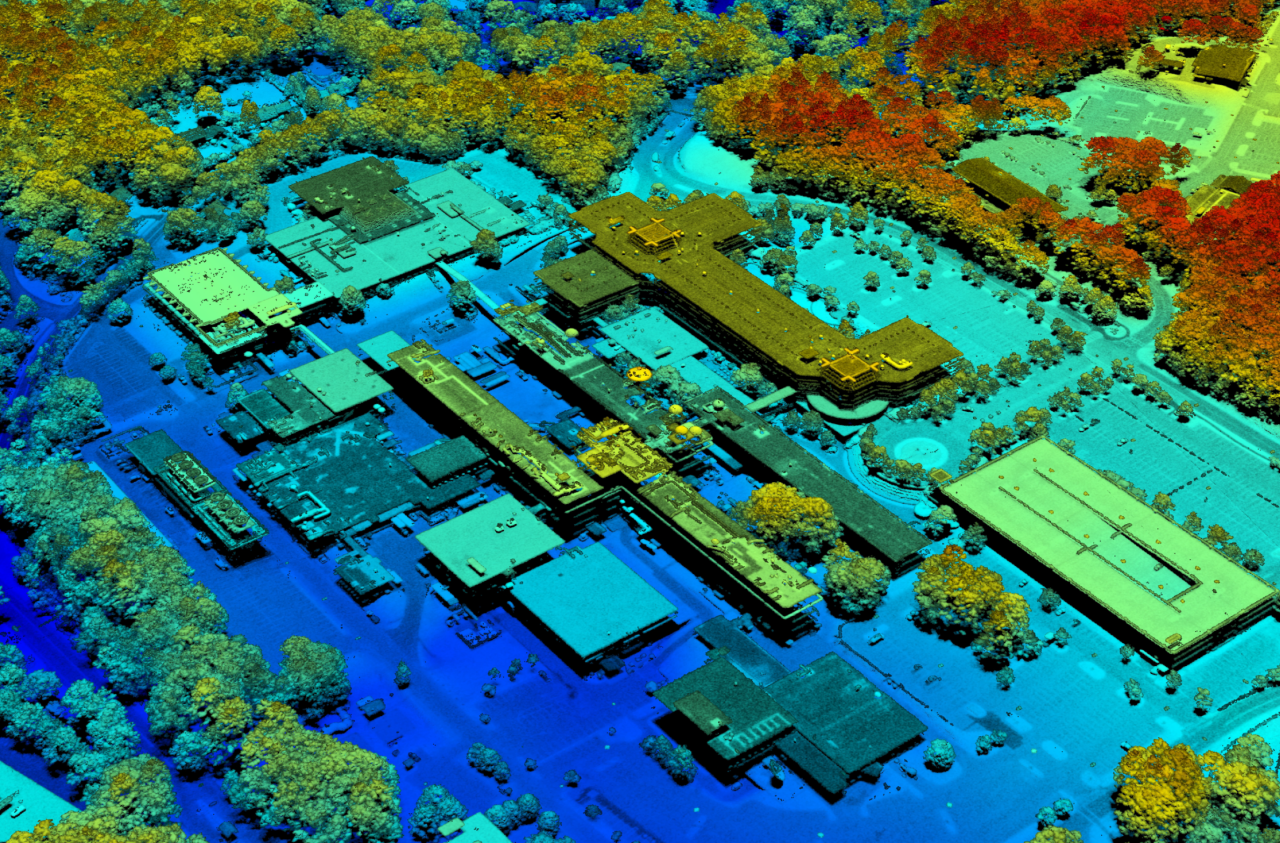
Compound Semiconductor Laboratory–Microsystem Integration Facility (CSL–MIF)
The CSL-MIF will provide 160,000 square feet of cleanroom space for developing complex electronic prototypes for DoW systems. Scientists and engineers will fabricate semiconductors made of two or more elements (compound semiconductors) and package specialized heterogeneously integrated electronics. Integrating different semiconductor materials and devices enables customizable microsystems for varied applications. Focus technologies include 3D-integrated focal plane arrays for surveillance, electro-optical systems for space-based optical communication, and superconducting microsystems for quantum computing. The CSL-MIF will complement our existing Microelectronics Laboratory, the U.S. government's most advanced silicon-based research facility.
Engineering Prototyping Facility (EPF)
The EPF will provide 290,000 square feet of infrastructure to support all phases of rapid and complex prototype development. Engineers and technicians will use this integrated space to design, simulate, fabricate, integrate, and test next-generation systems. Key spaces include assembly and integration labs, mechanical and electronic fabrication shops, vibration and environmental test labs, and secure prototyping spaces. Its flexible layout will accommodate work on emerging technologies while allowing rapid response to DoW prototyping needs.
As we mark 75 years of impact in 2026, our work for the nation continues.
Stay connected with MIT Lincoln Laboratory