
Test Agreements
If you are ready to test or validate your technology but are unable to access test facilities in the private sector, consider entering into an MIT Lincoln Laboratory test agreement that will allow your technology to be tested in the Laboratory's state-of-the-art facilities.
The Laboratory can perform testing for an interested party in its facilities on a reimbursable basis. Testing may include, but is not limited to, materials, equipment, models, and computer software. Under these agreements, Lincoln Laboratory does not perform any research or development. All test data belong to the customer. Please note that Lincoln Laboratory cannot directly compete with domestic private sector companies that also provide such testing capabilities. For further guidance, please contact the Laboratory's Compliance and Contracts Office.
To view a sample of a test agreement with Lincoln Laboratory, please view the drafted example below.
Available Lincoln Laboratory testing facilities
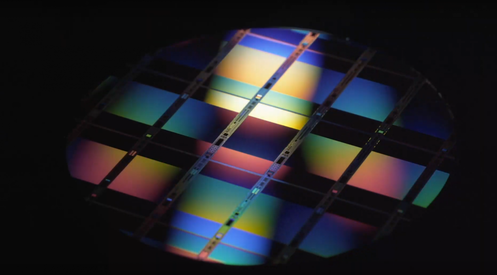
Microelectronics Laboratory
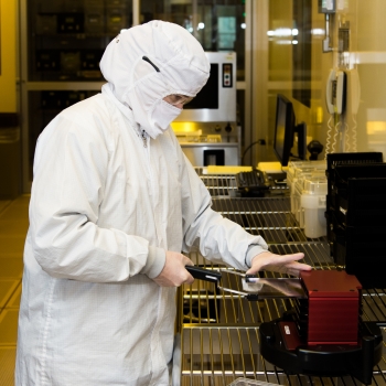
This 90-nanometer semiconductor research and fabrication facility is the most advanced foundry within the U.S. government's FFRDC network, including DoE national laboratories, DoC laboratories, and DoW service laboratories. Its production-class CMOS toolset allows the fabrication of 90-nm FDSOI CMOS, scientific-grade charge-coupled-device (CCD) imagers, digital superconducting circuits, and photonic integrated circuits. We have lithography platforms for 193-nanometer scanning, 248-nanometer and ultrawide-field I-line stepping, and 4-nanometer electron beam writing. A molecular-beam epitaxy system can provide high-sensitivity and highly stable back-illuminated devices in the ultraviolet and extreme ultraviolet ranges. Access to our highly capable and well-controlled 200-millimeter wafer fabrication services is possible through a test agreement or a more traditional Cooperative Research and Development Agreement.
This laboratory has Category 1-A Trusted Design; Aggregation; Foundry Services; Post Processing; and Packaging/Assembly, accreditation from the DMEA (Defense Microelectronics Activity), and ISO 9001:2015 Certification.
Explore how MEL's advancements can power the future of technology—your partnership and insights might be key to shaping what’s next! Email [email protected] to connect.
More on the Microelectronics Laboratory
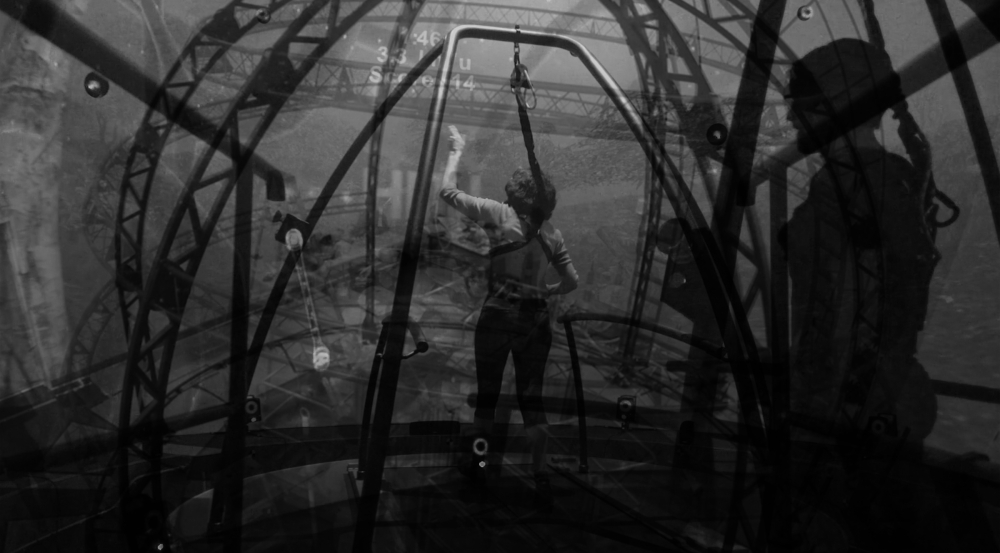
Sensorimotor Technology Realization in Immersive Virtual Environments (STRIVE) Center
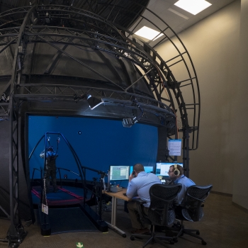
This research facility features a 24-foot virtual reality dome, the Computer Assisted Rehabilitation Environment (CAREN), one of only three full-dome CAREN systems in the world. In the CAREN, a user is immersed in a simulated environment that is displayed on a 360-degree screen and whose 6-degrees-of-freedom motion platform can mimic the environment's terrain. The center's multimodal suite of laboratory-grade instrumentation is used for quantifying human body biomechanics, ground reaction forces, electrophysiological signals, and vital signs.
Researchers in the STRIVE Center have developed several immersive virtual environments for the CAREN, including ones that allow operational testing and evaluation of wearable devices and military gear and ones that enable static and dynamic balance testing of individuals with neurological impairments. Virtual environments can be developed and customized to meet the needs of test agreement partners.
For information on how to work with the STRIVE Center to advance your research, email [email protected].
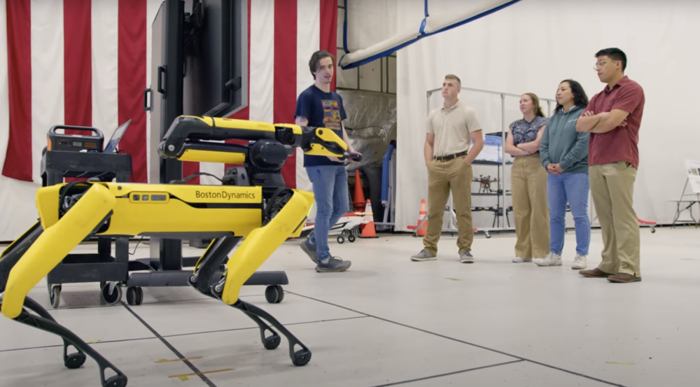
Autonomous Systems Development Facility (ASDF)

This state-of-the-art resource enables the development and testing of autonomy algorithms and capabilities in unmanned air and ground vehicles. At 17,000 square feet with greater than 30-foot flight clearance, this space is one of the world's largest indoor UAV testing facilities with full-coverage motion capture. We can accommodate the prototyping and testing of ground-based, aerial, and undersea autonomous systems. Vertically retractable nets provide safety barriers and act as dividers to allow multiple programs to use the facility at the same time. Simultaneous multi-angle and high-speed video recording are available to document tests.
For information on how to work with the Autonomous Systems Development Facility to enhance the development of your systems, email [email protected].
Radio-Frequency Systems Test Facility (RFSTF)
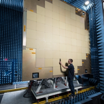
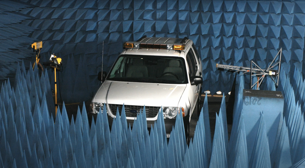
This research and development facility is a full-function rapid prototyping environment with resources for designing, fabricating, and measuring antennas and radar targets for surface, airborne, and space applications. The RFSTF contains six shielded anechoic chambers, a system integration lab (SIL), a high-bay staging area for rapid prototyping, and an RF laboratory. Mobile test vans and trailers are also available.
The anechoic chambers enable antenna, radar cross-section, and system tests and measurements over a wide frequency range and can accommodate test articles weighing up to 2000 lb. The large near-field scanner chamber is configured to measure large phased array antennas and reflector antennas while the small near-field scanner chamber is used to calibrate and test phased array antenna panels and small reflector antennas. To support chamber measurements, the general-purpose RF laboratory provides bench space and equipment, including network analyzers, spectrum analyzers, oscilloscopes, and signal sources. The SIL contains test equipment for rapidly prototyping and/or integrating systems before they are fully deployed and tested in the field, and accommodates a wide range of AC-power requirements. The rapid prototyping shop offers many machining tools to fabricate antennas, target-mounting fixtures, and other mechanical pieces necessary for testing in the facility. The shop's high-bay area with an overhead crane permits mechanical work on large systems.
More detailed information about this facility can be found in the RFSTF brochure.
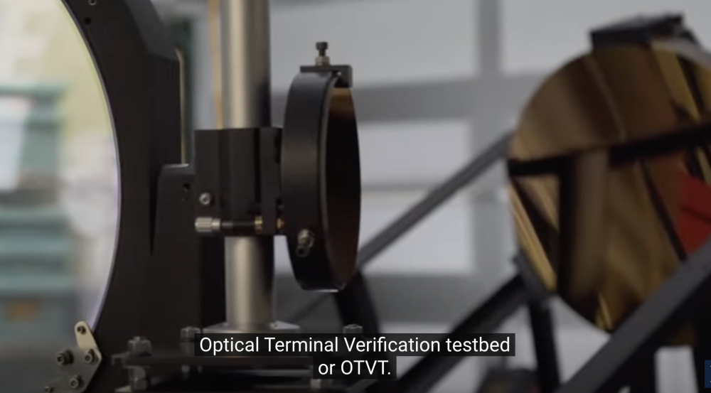
Optical Terminal Verification Testbed (OTVT)
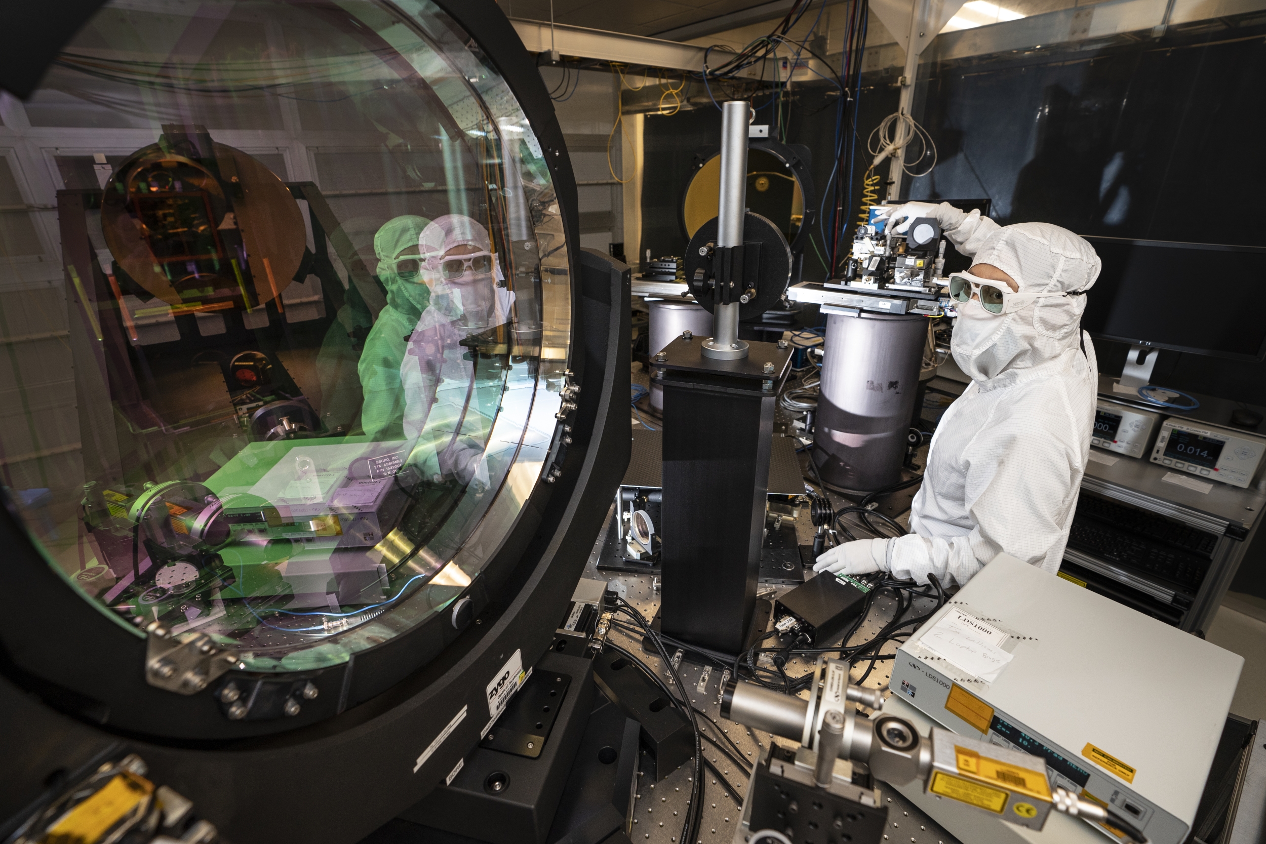
Lincoln Laboratory's Optical Terminal Verification Testbed (OTVT) is a premier laboratory for evaluating terminals for free-space laser communications (lasercom). It was built to fill a national capability gap: the need for a facility and an experienced team to provide trusted, unbiased assessments of the capabilities of lasercom terminal prototypes.
The OTVT enables developers of lasercom terminals to conduct both functional and quantitative tests, including basic optical characterization, link acquisition and tracking, and communications performance. It offers a setting in which engineers have precise control over the execution of all tests, allowing them to isolate specific effects and evaluate their impacts on terminals. This laboratory testing also helps developers identify limitations of their terminal hardware and software, allowing them to make and verify improvements to their designs early in the development cycle.
The OTVT facility includes a cleanroom with stable temperature control, humidity monitor, laminar air flow to minimize unintended turbulence effects, and separate areas for terminal operation and testbed control. Automated testing control assures precise, accurate, and repeatable results. Engineers can take advantage of the OTVT's high-performance optics and sensors to accurately measure a terminal's optical beam quality, an assessment crucial for understanding the system's far-field performance. High-rate data sampling allows playback and detailed analysis of spatial acquisition and tracking after the fact. For communications testing, the OTVT has two sets of modems, one for assessing a system's functional interoperability and one for precisely characterizing waveform performance. Fiber-coupled communication hardware allows easy reconfiguration for different waveforms. During test events, developers can observe test telemetry in real time while listening to audio from the testing team.
To help developers understand how a terminal will operate in the field, the OTVT can emulate various link conditions of the terminal's intended environment:
- Far-field intensity and phase of the beam from the remote terminal
- The remote terminal's pointing, acquisition, and tracking (PAT) sequence, including propagation delay
- Residual line-of-sight jitter of the local host platform
- Fading caused by both turbulence and dynamic pointing errors
- Point-ahead angle
- Doppler shift
Since beginning operation in 2005, the OTVT team has conducted more than 20 formal test events. The facility has hosted multiple industry teams, supported several internal efforts, and contributed to NASA lasercom demonstrations, such as testing optical modems for its Laser Communications Relay Demonstration and providing camera algorithms for pre-launch testing the Lunar Atmosphere and Dust Environment Explorer satellite. A major hardware and software refresh was completed in 2019.
In the next decade, interest and growth in the lasercom industry is expected to create concurrent, rapid U.S. lasercom terminal production within the defense industrial base. The OTVT will continue to advance cutting-edge lasercom solutions, helping developers create innovative terminal designs and informing U.S. government acquisition teams on the viability of new lasercom systems.
For information on how to work with the Optical Terminal Verification Testbed to enhance the development of your systems, email [email protected].