
Microelectronics Laboratory
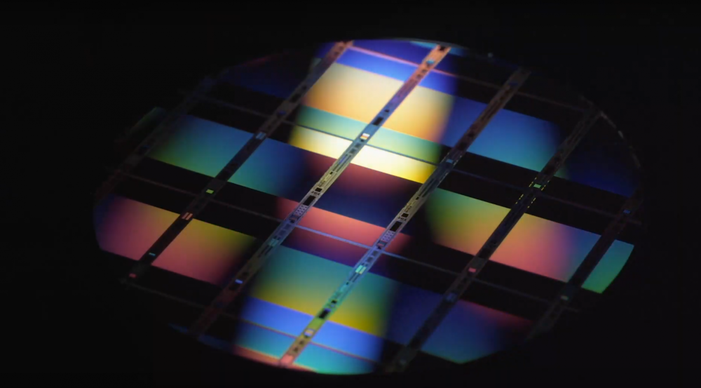
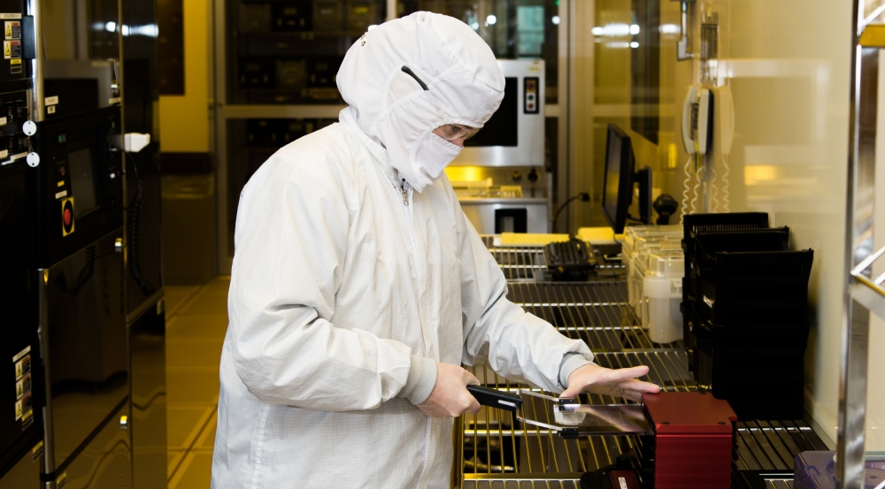
The MIT Lincoln Laboratory Microelectronics Laboratory is the U.S. government's most capable semiconductor research and fabrication facility. This 70,000-square-foot facility has 8,100 square feet of class-10 and 10,000 square feet of class-100 cleanroom areas to support a wide range of Lincoln Laboratory programs.
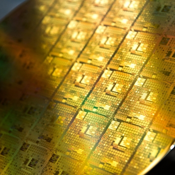
The 200-mm wafer equipment is continually updated and includes a production-class complementary metal oxide semiconductor (CMOS) toolset with angled ion-implantation, cluster metallization, and dry etch equipment; chemical-mechanical planarization equipment; and rapid thermal processing and advanced lithography capabilities. A molecular-beam epitaxy system is used to provide high-sensitivity and highly stable back-illuminated devices in the ultraviolet and extreme ultraviolet ranges.
Currently, staff in the Microelectronics Laboratory are developing and fabricating novel technologies, including the following:
- A fully depleted silicon-on-insulator (FDSOI) CMOS circuit prototyping capability with extreme environment variants, including radiation hardness
- Flight-quality gigapixel charge-coupled-device (CCD) imager focal planes and photon-counting avalanche photodiode arrays
- Niobium-based superconducting circuits
- Photonic integrated radio-frequency and optical microelectromechanical systems (MEMS)
- Gallium nitride on silicon high-electron mobility transistors (GaNSi HEMTs) and circuits
In addition, the Microelectronics Laboratory supports advanced packaging with a precision multichip module (MCM) technology and an advanced three-dimensional circuit stacking technology.
More than 40 different programs from divisions at Lincoln Laboratory, as well as from industrial sponsors involved through cooperative research and development agreements, are supported by the Microelectronics Laboratory.
The Microelectronics Laboratory is staffed by approximately 60 technicians, engineers, and scientists. This facility is operated in three shifts each day, five days a week.
The Microelectronics Laboratory has Trusted Foundry accreditation from the DMEA (Defense Microelectronics Activity) and ISO-9001 certification.
Read an overview of the benefits the Microelectronics Laboratory has on our R&D and the unique tools it offers.
Microelectronics Laboratory Capabilities
Microelectronics Laboratory Facility Brochure
See our fact sheets below on recent innovations enabled in this laboratory.
Fully Depleted Silicon-on-Insulator CMOS
GaN-CMOS Wafer-Scale 3D Integration
Microhydraulic Actuator Development
Silicon & Silicon Nitride Integrated Photonics
Superconducting Integrated Circuits
A commemorative booklet highlights 20 important innovations that have been enabled by the facilities within this lab.
20 Innovations over Twenty Years
For more information about the Microelectronics Laboratory and its capabilities, contact [email protected].