
Facilities
Tagged As
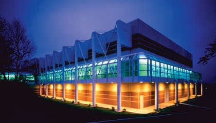
Electronic-Photonic Integration Facility
MIT Lincoln Laboratory
The state-of-the-art facility supports the development of optoelectronic components, photonic integrated circuits, CMOS electronic integrated circuits, and hybrid electronic-photonic integration techniques.
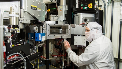
Microelectronics Laboratory
MIT Lincoln Laboratory
The Microelectronics Laboratory is a state-of-the-art semiconductor research and fabrication facility that supports the design, fabrication, and packaging of novel devices.
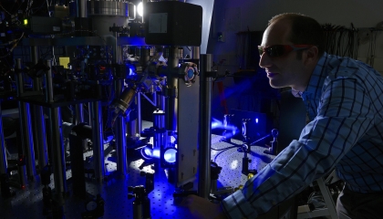
Quantum Computing Laboratory
MIT Lincoln Laboratory
We are studying methods to use trapped ions and Josephson junction–based superconducting circuits for large-scale quantum information processing.