
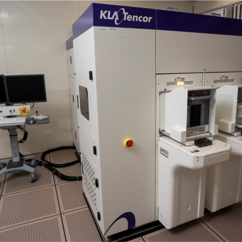
- 90 nm resolution
- 20 nm overlay (8-nm upgrade in progress)
- 26 mmx32 mm (scan) field size
- Four-times reduction, 0.75NA lens
- Interfaced to TEL ACT12 track for full-flow lithography
- Focus spot monitor and EFESE upgrades
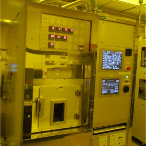
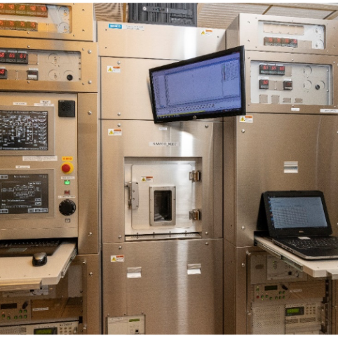
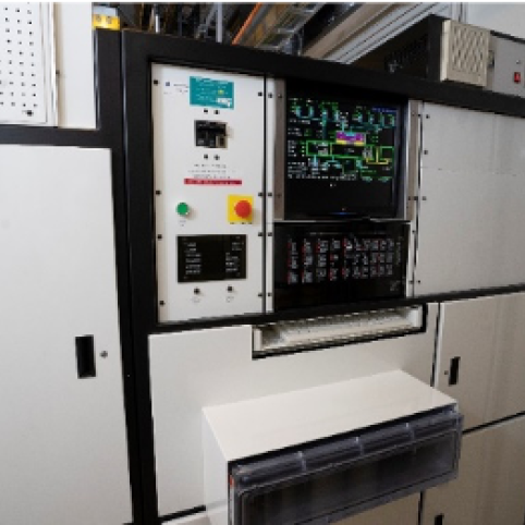
Fabrication
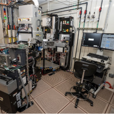
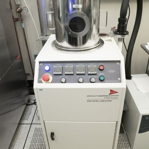
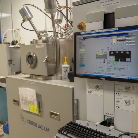
200-Millimeter Wafer Fabrication
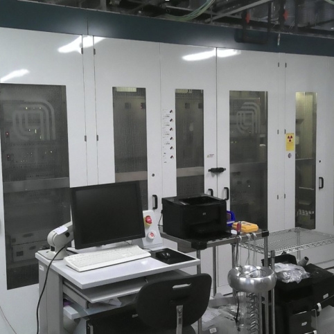
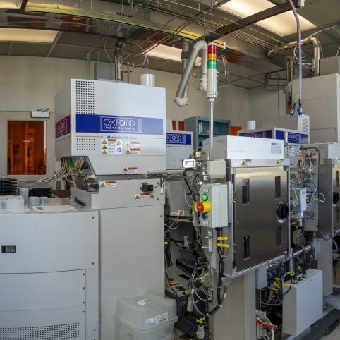
Fabrication and integration capabilities are enabled by the Microelectronics Laboratory (ML), a 200 mm wafer processing facility equipped with commercial-class cassette-to-cassette fabrication equipment and professionally staffed 24 hours a day, five days a week. This 90 nm-class facility operates full-flow fabrication across a broad range of integrated circuit technologies, including fully depleted silicon-on-insulator CMOS, CCD imagers, superconducting electronics, photonics, MEMs, and microfluidics.
Our versatility is enabled with i-line, 248 nm, and 193 nm projection lithography platforms, along with direct-write electron beam and laser systems. We stitch exposure fields within and across lithography platforms, providing very-large-device capabilities.
The ML is well suited for prototyping work needing large wafers, lots of small features, and process control systems to demonstrate uniformity, repeatability, process integration, or other commercial insertion risk reduction.
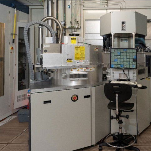
Lithography

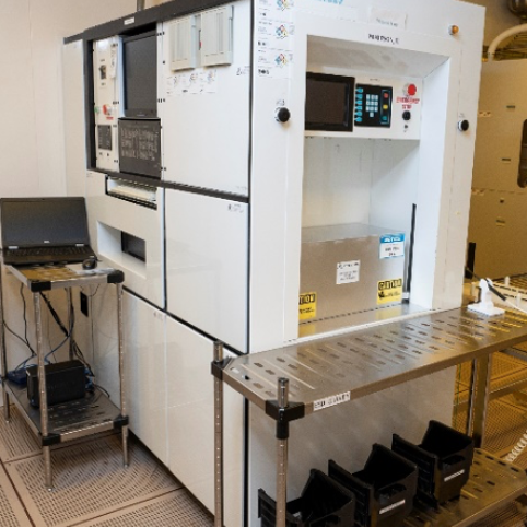
193 nm ASML PAS5500/1100 Scanner

365 nm Canon iW Wide-Field Stepper
- 800 nm resolution (600 nm demonstrated)
- 150 nm overlay
- 50 mmx50 mm field size
- Two-times reduction, 0.27NA lens
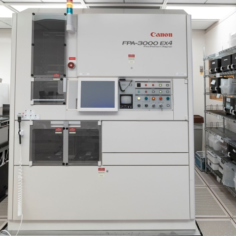
248 nm Canon EX4 stepper
- 250 nm resolution (200 nm demonstrated)
- 100 nm overlay
- 22 mmx22 mm field size
- Five-times reduction
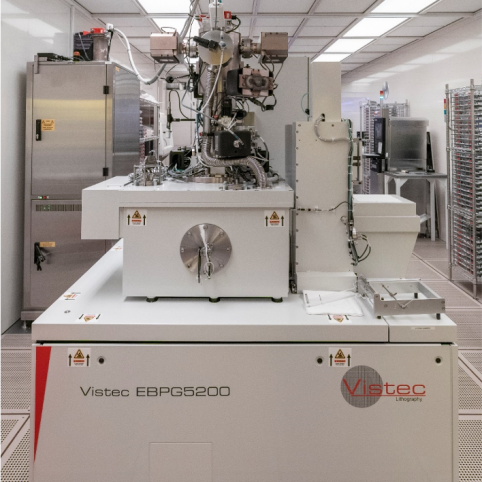
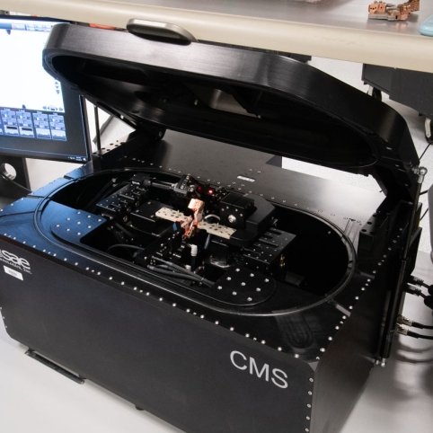
Raith EBPG 5200 Scanning Electron-Beam Lithography
- High-resolution lithography with 7 nm spot size
- 100 kV write mode
- 200 mm wafer through part piece compatibility
- Automated exposures from 10 holder loadlock
- GenISys BEAMER and Raith GUI combine for advanced pattern preparation

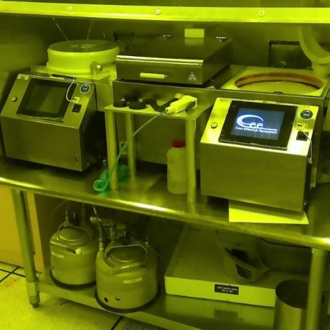
Hitachi CDSEM S-9300 Electron Microscope
- 200 mm field emission top-down critical dimension (CD) SEM
- Dual load ports
- Dual load chamber
- Resolution < 80 nm
- Auto job CD measurements
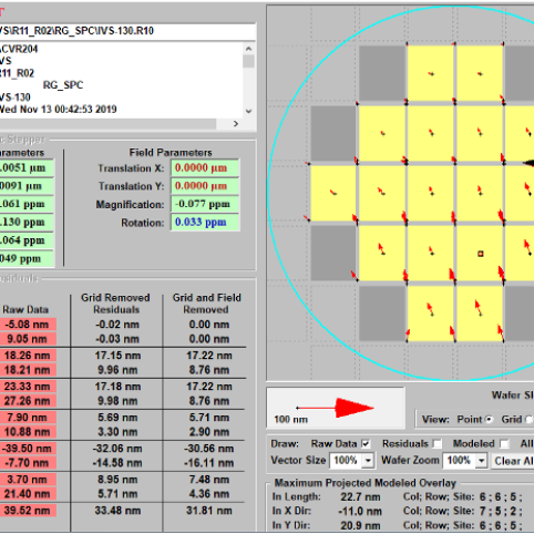
IVS-130 Optical Overlay Metrology
- 8 nm resolution
- 200 mm system with three indexers
Etch
AMAT Centura Etchers – Front End (FE) and Back End (BE)
- DPS Poly (FE) – ICP etcher used for HBr/Cl2–based Si etches
- DPS Metal (BE) – ICP etcher used for Cl2/BCl3–based AlCu stack and other metal etches
- EMAX CT+ (FE and BE) – MERIE etcher used for fluorocarbon-based dielectric etches
- ASP+ (FE and BE) – Downstream microwave strip chamber for O2/H2O–based in situ resist strip
Lam Alliance Deep Silicon Etch
- High Si etch rate ~2–3 µm/min
- High aspect ratio up to 100:1
- High selectivity to resist mask (100:1) and oxide hardmasks (200:1)
Samco RIE-200 Oxide Etch
- 200 mm cassette to cassette
- Dielectric fluorocarbon etches
Samco RIE-200 Metal Etch
- 200 mm cassette to cassette
- 2-chamber cluster
- Cl2/BCl3–based metal etches
- In-situ O2/NH3 resist strip
Mattson ICP Resist Strip
- O2 remote plasma
- 250C post-implant resist strip
Mattson Triode
- O2 plasma with no bias
- 120C post-develop descum
- Good for limited thermal budget
Deposition

AMAT Endura
- Physical vapor deposition (PVD) sputtering
- Metal organic chemical vapor deposition
- IMP (Ionized Metal Plasma) sputtering
- Reactive PVD and IMP sputtering
- Orienter/Degas module
- Argon Sputter Preclean module
- Cool chamber

Electrotek Sigma Metal Deposition
- Al-based cluster metallization system
- Degas module
- Argon sputter pre-clean module
- Physical vapor deposition
- Reactive physical vapor deposition
Novellus Altus tungsten
- Tungsten deposition for damascene plug fill
- Chemical vapor deposition mode
- Pulsed nucleation layer mode

Wordentec Evaporator
- Six 200 mm wafer batch size
- Six-pocket electron-beam source
- Resistance thermal source
- Many established deposition materials
- Lift-off and other low-energy deposition processes
Novellus Speed + Sequel cluster
- Speed chamber has PECVD gap-fill deposition with simultaneous etch
- Sequel chamber has PECVD deposition of SiO2, Si3N4, SiOxNy
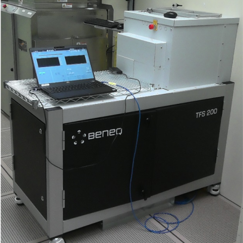
Beneq TFS-200 Atomic Layer Deposition
- Batch hot-wall reactor for high uniformity
- Demonstrated low-particulate films
Implant
High Current Ion Implanter
- Implant range: 5e12 to > 1e17 ion/cm2
- Wafer twist and tilt control
- 200 eV to 80 kV ion energy
- Species include phosphine PH3 (SDS) P+, P++, P+++; arsine AsH3 (SDS) As+, As++; boron trifluoride (SDS) BF3, BF2, B+, B++, F+; germanium tetrafluoride GeF4 (SDS) Ge4
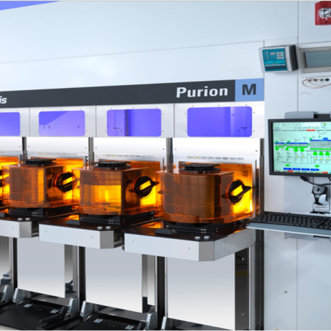
Purion MTM Single Wafer Medium Current Ion Implanter
- Mechanically limited throughput (200 mm): 425 WPH (single step)/320 WPH (quad mode)
- Dose range: 1.0E11–1.0E16 atoms/cm.
- Energy range of 2 keV to 1 MeV, single charge maximum of 335keV
- Programmable tilt, twist, and control
- Species include P+, P++, P+++, As+, As++, B+, B++, Bf2, GeF4

Applied Materials Radiance Rapid Thermal Processor
- Honeycomb lamp source
- Seven-point temperature measurement
- 100 Hz closed-loop control
- 240 rpm wafer rotation
- High uniformity spike anneal or implant and other anneals
Planarization
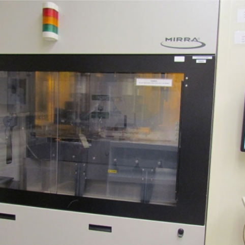
Applied Materials Mirra 3400
- Contour polish heads
- Five-zone “EZ UPA” head pressure control
- Timed oxide polish for intermetal dielectrics and ultra-shallow trench isolation
- End-pointed tungsten plug polish for damascene via interconnect
OnTrak DSS200 Wafer Scrubber
- Both-side polypropylene brush scrub
- Chemistry dispense
- Meg transducer in spin station
- Spin station and infrared lamp for wafer dry
Metrology
KLA 8920 Patterned Optical Defect Inspection
- Brightfield and darkfield imaging detection
- 35-times magnification
- ≤ 150 nm defect detection capability
- 20 wafers per hour at highest sensitivity setting
- On-board optical defect imaging
- Defect image throughput of 1.2 seconds per defect
- KLARF maps for electron microscope defect location
Hitachi 7840 Electron Microscope with Energy Dispersive Spectroscopy (EDS)
- Tip/tilt sample manipulation
- Profile and sidewall analysis
- Defect metrology
- Elemental analysis via Oxford Instruments EDS
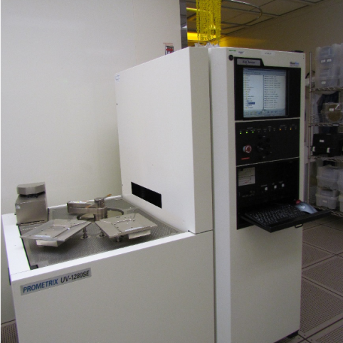
KLA UV1280SE Optical Film Thickness
- Thin film thickness, refractive index (n) and absorption coefficient (k)
- Dual beam spectroscopy – normal incidence
- Spectroscopic ellipsometry
- Film stacks up to 8 layers with 7 unknowns (t, n, or k)
- 250 nm to 800 nm λ lamp
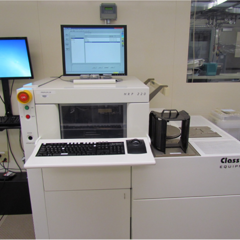
KLA HRP220 Profilometer
- Cassette to cassette
- Pattern recognition
- 10 nm to 131,000 nm step heights
- Static step height repeatability
- Static (no unload) 0.75 nm (1δ) on 1 µm step
- Dynamic step height repeatability (load and unload) 2 nm (1δ)
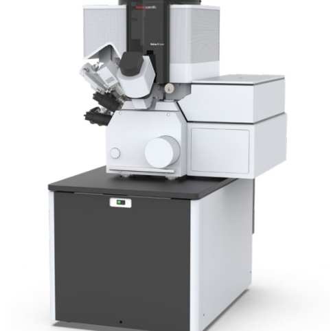
Thermo Fisher Helios 5 Focused Ion Beam Scanning Electron Microscope
- Cross-beam system with coincident electron and gallium ion beams
- 65 nA maximum focused ion beam current
- Sub-nm scanning electron microscope resolution at 1 kV
- Dual-wavelength femtosecond laser ablation system with < 300 fs pulse duration
- Multi-gas injection system for both metal/insulator deposition and accelerated etching
Wafer Bond

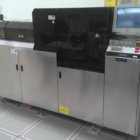
Disco DFD6240 Edge Trim and Wash
- Low trimmed edge roughness for reduced defect shedding
- Integrated spin rinse station
- Automated wafer on tape handling
- Automated wafer alignment
150-Millimeter and Below Wafer Fabrication
We design, grow, fabricate, and integrate discrete and arrayed electromagnetic sources and detectors in gallium arsenide, indium phosphide, and piezo systems, accommodating materials incompatible with silicon integrated-circuit production on a size-flexible tool set for wafers up to 150 mm, with many also capable up to 200 mm. These tools span lithography, etch, deposition, and metrology, enabling agile research and device development and fielding of prototype systems.
Lithography
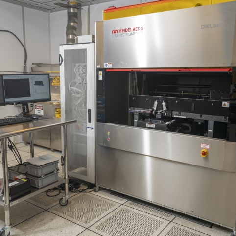
Heidelberg DWL 66+
- Exposure area up to 200 × 200 mm²
- Minimum feature size to 300 nm
- Maximum write speed of 2000 mm²/min (4 µm feature size)
- Address grid down to 5 nm
- Grayscale exposure mode with up to 1000 gray levels
- Front and backside alignment
- Climate chamber
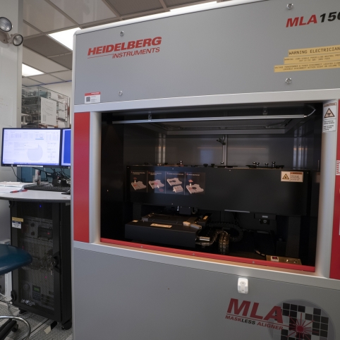
Heidelberg MLA150
- Direct-write laser system
- Automated stage
- Advanced laser focus
- .8 µ capability
- Backside alignment
Suss RCD8 Coaters and Developers
- Edge bead removal, back-side rinse
- Bulk and cartridge-based automated dispensing systems
- Gyrset option for rectangles and viscous coatings

Adhesion Vapor Prime Treatment
- HMDS priming
- N2 flushing program controlled, no oxidation
- Heating ramp-up with 20 program-steps

Sheet Resist Laminator
- 200 mm resist laminator
- Wide variety of thicknesses
Brewer 200 mm Spin Coater and Bake
- Automated recipe control
- Spin, exhaust control options
- Bake plate, programmable lift pins
Low-Energy Deposition Systems

Temescal 2500 E-Beam Evaporator
- Electron beam evaporator
- Six 15 cc pockets
- Advanced sweep
- Large batch, up to four 200 mm wafers
- Rotation
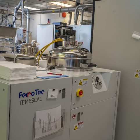
Ferrotec FC-2000 E-Beam Evaporator
- Dielectric
- Four 25 cc pockets
- PopTop source
- Ion beam
- Load locked
- Variable angle planetary
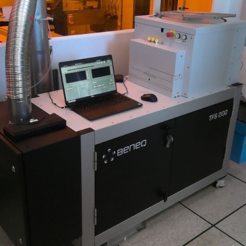
Beneq TFS200 Atomic Layer Deposition
↵
- High aspect ratio fill
- Load locked
Electroplating
- 200 mm wafers or smaller
- Fountain plate design
- Copper 500 µm deposition
- 200 µm conformal fill
Parylene Deposition
- Pulsed flow exothermic silicon and germanium etching
- Manual load workpieces of 200 mm wafers and smaller discrete items
Other Deposition Systems

Samco PECVD
- Oxides and nitrides
- Six-gas plasma-enhanced chemical vapor deposition, including tetraethyl orthosilicate
- 50–300 C electrode temperature control
Unaxis PECVD
- Oxides and nitrides
- Six-gas plasma-enhanced chemical vapor deposition
- Temperature-controlled upper/lower electrodes
Denton Discovery Sputterer
- Four sources: three DC sources (metal) and one RF source (insulators)
- Pre-clean RF
- Load lock
AJA Combinatorial Sputter System
- Four simultaneous sputter sources
- E-beam evaporator
- Indexing sputter mask for same-run experimentation
Dry Etch Systems
Oxford Cluster ICP
- Three-chamber inductively coupled plasma cluster etch system
- 2 in to 200 mm capable
- Advanced endpoint
- Backside helium cooled
- Load locked cassette-to-cassette loading
Samco ICP (2X)
- 150 mm capable
- Load locked
- Electrostatic chuck
- Backside helium cooled
- 250 C electrode temperature
Samco 10NR RIE
- Highly selective anisotropic etcher
- Silicon, silicon dioxide, polysilicon, silicon nitride, gallium arsenide
- 1 kW RF generator
- Water-cooled platen
AJA Ion Beam Assisted Etch
- Ion milling process
- 50–1200 eV
- Profile +/-2%
- Cooled substrate
- Load locked/silicon dioxide
- Precision tilt angle
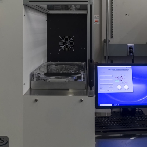
XeF2 Etch
- Pulsed flow exothermic silicon and germanium etching
- Manual load workpieces of 200-mm wafers and smaller discrete items
Metrology Systems

Film Sense Multiwavelength Mapping Ellipsometers
- Six wavelengths, 405–950 nm spectral range
- Wafers to 300 mm
- Automated user-defined mapping measurements
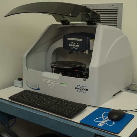
Mapping Profilometers
- Manual load mapping profilometers include Dektak XT, Tencor P-17, and Tencor P-15
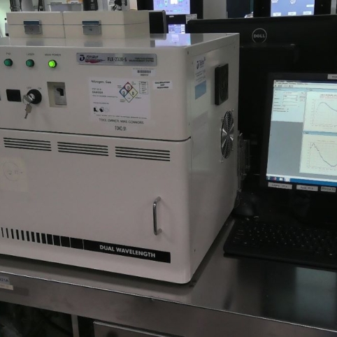
ToHo FLX Film Stress Measurement
- 50–200 mm wafers
- Precision wafer bow from laser reflectance
- Stress range of 1–4000 MPa
- Accuracy of < 2.5%
- Room temperature to 500 C operation
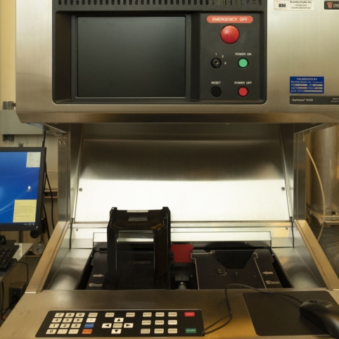
Tencor Surfscans
- Measures 50–200 mm wafers
- Defect sensitivity of 0.23 µm
- Defect map and histogram with zoom
- Haze map and histogram with zoom

View Critical Dimension Measurement
- Automated critical dimensions and overlay measurement
- Width accuracy to 500 nm
- Overlay accuracy within 50 nm
- 200 mm mapping stage
- Automated imaging documentation
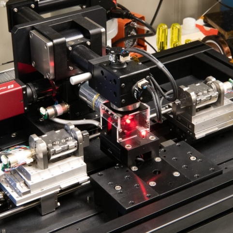
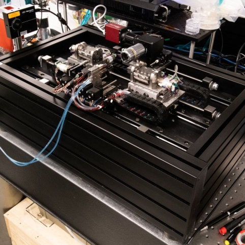
Fiber-Optic Research and Prototyping
We aim to advance the state of the art in fiber-optic processing, fiber components, and glass-based optical devices. Many of our efforts involve the boundary between fiber optics and free-space (for example, fiber laser endcaps and monolithically integrated lensed fibers).
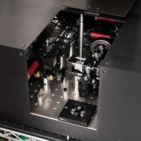
We have equipment and processes capable of producing devices with tight specifications on wavefront quality (for applications such as interferometry or free-space optical communication) as well as ultra-low-loss devices capable of operation at the multikilowatt power level. We have equipment capable of stripping, cleaning, cleaving, and splicing optical fibers and other glass structures from 80 μm to 3 mm in diameter. We also own equipment capable of changing the mode field diameter of fibers by tapering or thermally diffusing the core, as well as the ability to machine the cladding into different shapes or etch features into the cladding. Tapering operations are one of the fundamental processes involved in the fabrication of fused fiber couplers and pump/signal combiners used in optical fiber amplifiers.
A suite of metrology equipment is also available, including 2D refractive index and dopant profiling of fibers as well as accurate measurement of modal properties, beam quality, polarization quality, and wavefront.
Advanced Fiber and Glass Processing
3SAE Technologies Combiner Manufacturing System
- 3-electrode arc discharge splicer, can operate in partial vacuum for lower heat levels, improved power uniformity
- Can splice optical fiber from 80 to 2500 μm cladding diameter
- Tapering operations with process monitor
- Thermal core expansion
- In-situ fiber cleaver
- Polarization-maintaining fiber rotational alignment capability (manual, end view only)
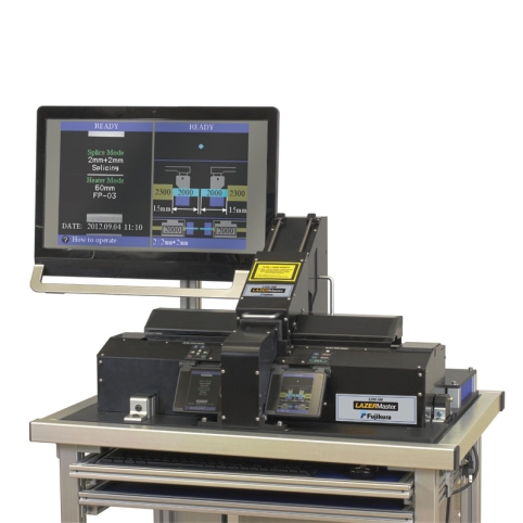
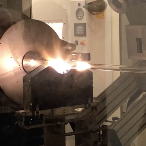
Fujikura LZM-100 CO2 Laser-Based Glass Processing System
- Uses absorption of CO2 laser light (~10 μm wavelength) to splice fibers up to 2.3 mm cladding diameter
- Light-tight (class 1 laser product)
- Tapering and thermal core expansion operations
- Polarization-maintaining fiber rotational alignment capability (end view or side view)
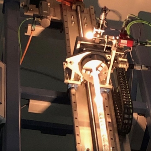
SubMicron Engineering CO2 Laser-Based Fiber Machining System (FMS)
- Uses absorption of CO2 laser light (~10 μm wavelength) to thermally ablate glass cladding material without substantially weakening fiber
- Light-tight (class 1 laser product)
- Fiber rotation allows for machining of cladding anywhere on azimuth
- Capable of machining along fiber length up to 12 cm
SubMicron Engineering Combiner Fabrication System
- Oxyhydrogen flame-based splicing and glass processing system with flexible torch design
- Can splice optical fiber from 80 μm to greater than 2.5 mm diameter
- Tapering and thermal core expansion operations
- Polarization-maintaining fiber rotational alignment capability (end view only)
- In-situ fiber cleaver and fiber recoater
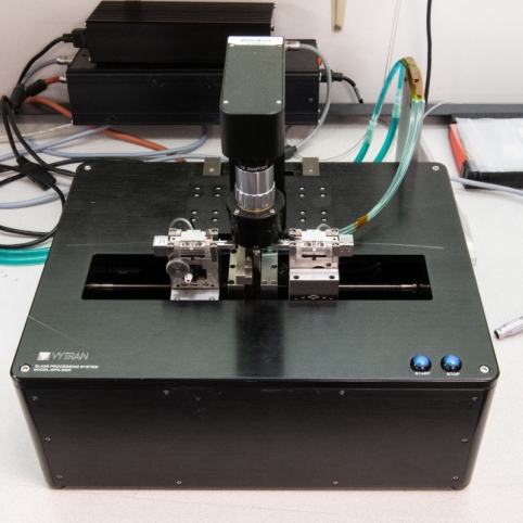
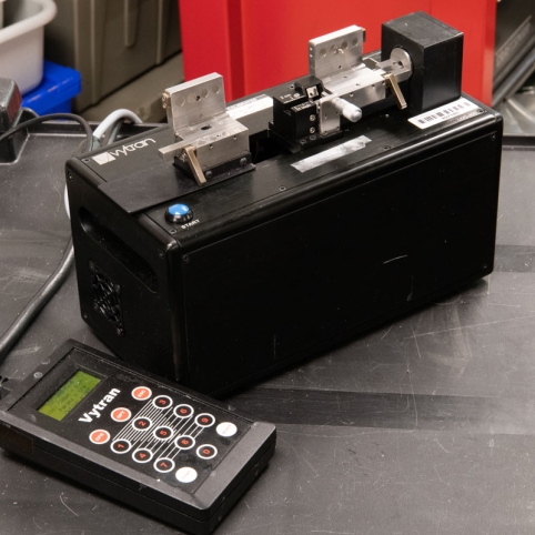
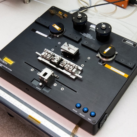
Vytran GPX-3600 Glass Processing System
- Filament fusion splicing and glass processing system
- Can splice optical fiber with cladding diameters up to 1.7 mm
- Tapering and thermal core expansion operations
- Polarization-maintaining fiber rotational alignment capability (end view only)
Fiber Cleaning
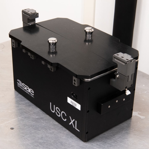
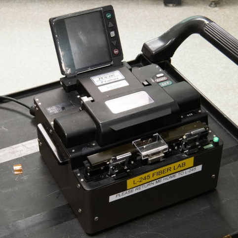
3SAE Technologies USC-XL Ultrasonic Cleaner
- Ultrasonic actuation of solvent bath removes residual acrylate coating left after fiber stripping
- Cleans fiber lengths of up to 200 mm
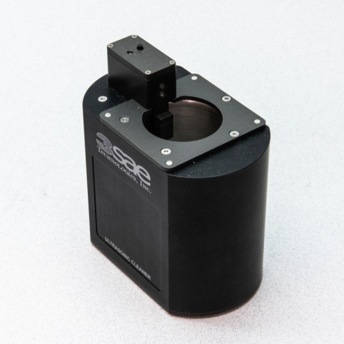
3SAE Ultrasonic Cleaner
- Ultrasonic actuation of solvent bath removes residual acrylate coating left after fiber stripping
- Compatible with Fitel and Fujikura fusion splicer fiber holders
Fiber Cleaving

Northlab Photonics ProCleave LD II
- Cleaves fiber with cladding diameters up to 550 μm
- Can be operated by using battery power
- Can store four separate cleave programs when disconnected from a computer
- Flat cleaves only
SubMicron Engineering Stress-Relieving Cleaver
- Cleaves fiber with cladding diameters up to 1000 μm
- Capable of < 0.1 degree cleave angles via relief of torsional clamping stress
- Flat cleaves only
Vytran LDC Cleaver
- Cleaves fiber with cladding diameters between 80 and 1000 μm
- Flat or angled cleaves

York FK11 (Flat) and FK12 (Angled) Fiber Cleavers
- Cleaves fiber with cladding diameters between 80 and 200 μm
- Battery operated
- Compatible with Fitel and Fujikura fusion splicer fiber holders
Fiber Proof Testing
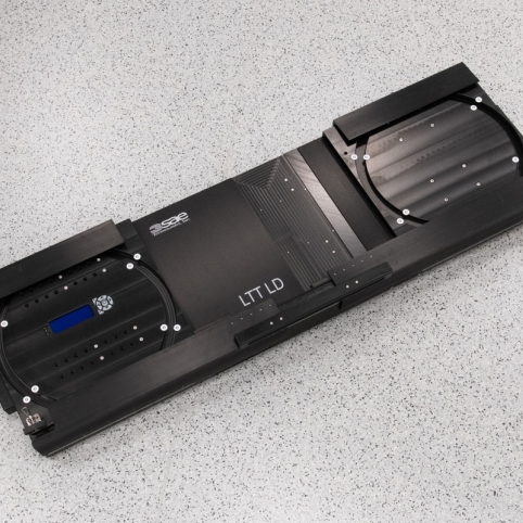
3SAE Technologies LTT-LD Proof Tester
- Up to 220 N of force
- 160–1000 μm fiber diameter (including coating)
Fiber Recoating

Vytran PTR Series Recoater
- 320 μm and 600 μm diameter recoat diameters
- Acrylate and fluoroacrylate coating materials
- Recoat lengths 50 or 100 mm (depending on model)
Fiber Splicing
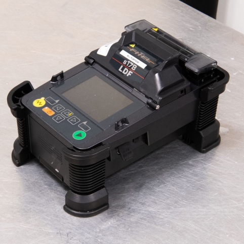
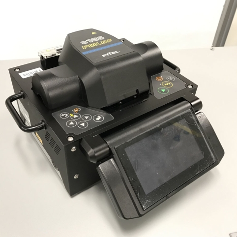
Fitel S178LDF
- Arc-discharge fusion splicer (2-electrode)
- 125–450 μm cladding diameters
- Can operate on battery power
Fitel S184PM
- Arc-discharge fusion splicer (3-electrode)
- Polarization maintaining fiber rotational alignment capability (side view only)
- 80–600 μm cladding diameters
Fitel S185PM-LDF/S185PM-ROF
- Arc-discharge fusion splicer (2- and 3-electrode models in house)
- Polarization-maintaining fiber rotational alignment capability (side view only)
- 80–800 μm cladding diameters (depending on model)
- Can operate on battery power
Fujikura FSM-100P+
- Arc-discharge fusion splicer (2-electrode)
- Polarization-maintaining fiber rotational alignment capability (end view and side view)
- 80–1000 μm cladding diameters
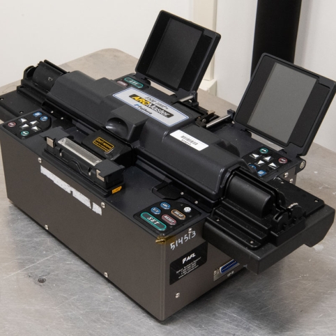
Vytran FFS-2000
- Filament fusion splicer
- Polarization maintaining fiber rotational alignment capability (end view only)
- Strips, cleans, cleaves, splices, and recoats fiber, all in one unit
- 80–200 μm cladding diameters
Fiber Stripping
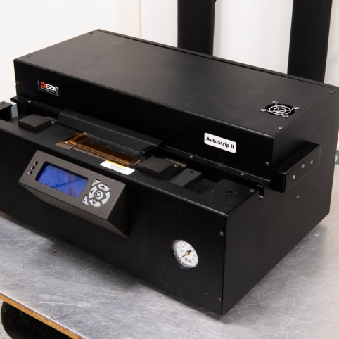
3SAE Technologies Autostrip II Thermal Fiber Coating Stripper
- Hot-air thermal fiber stripper for fibers with coating diameters up to 600 μm
- Fiber strip lengths 2–150 mm
- Window-stripping only (does not strip the ends of fibers)
Fujikura PCS-100 Stripper
- Motorized razor-blade stripper
- For fibers with cladding diameters between 60–1200 μm
- Fiber strip lengths 1–35 mm
Metrology
IFA-100 Refractive Index Profiler
- 1D and 2D refractive index profiling of 40–400 μm diameter optical fibers at wavelengths between 500 and 1000 nm
- 500 nm transverse spatial resolution, 10 μm axial resolution
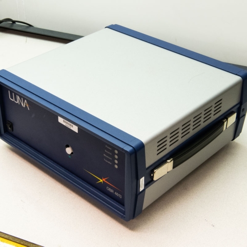
Luna Technologies Optical Backscatter Reflectometer
- Measures reflectivity vs. fiber length at 1310 or 1064 nm center wavelength via swept-wavelength interferometry
- 10 μm spatial resolution out to 30 m fiber length
Optical Coatings
We provide optical thin films ranging in application from the X-ray to the infrared. Each job encompasses consultation, design, manufacturing, and optical testing. We extensively use ion beam deposition for the lowest absorption/scatter and highest laser damage threshold coatings currently possible. We also modify processes to accommodate live experiments, unusual workpieces, and security-sensitive material.
Equipment

- Dielectric and metal beam splitters, polarizing beam splitters
- Black mirrors, hot mirrors, cold mirrors
- Antireflection coatings: single, multi, and broadband wavelength
- High laser damage reflectors, multichroic, laser chirped mirrors
- Neural density filters, forced absorbers
- Edge filters, long wave and short wave pass filters
- Narrow band pass filters: single- and multicavity, gain flattening
- Insulating films and spacer dielectrics with sub-nanometer-thickness control
- Metal films: Al, Au, Ag, Cr, Cu, Hf, Mo, Ni, Pt, Re, Ru, Ta, Ti, V, Zr
Defense Fabric Discovery Center
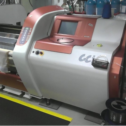
The Defense Fabric Discovery Center (DFDC) enables us to develop advanced fiber and fabric technology that can provide soldiers with wearable capabilities. This prototyping facility is equipped to design and produce fabrics with embedded microelectronics, enabling these fabrics to change color, store energy, emit and detect light, monitor health, or facilitate communication. The DFDC has CAD software for modeling the fiber preform that contains the microelectronics, draw towers to pull and spool the fiber, full-garment knitting machines to weave the fiber into fabric, and system integration technology to produce a finished product.
Equipment

Shima SWG 041 N2 Wholegarment® “Mini” Machine
- 10 needles/inch
- 8 yarn carriers
- 1 elastic yarn feeder
- 16 in knitting width designed for hats, gloves, and small swatches
- Yarn unwinding accessory for spooling fiber of flanged spools
CCI Studio Loom & Mini Lutan Warper
- Maximum fabric width: 20.5 in
- Maximum fabric length: 25 m per warp
- Servo-feeder for flange spooled fiber
- Rigid rapier loom
- Cut selvedge fringe on each side of fabric
- Yarns not continuous

Advantek Polymer Draw Tower
- Tower height: 6 m
- Draw speed up to 15 m/min
- Three zone furnace
- 50 mm inner diameter
- Individually controlled zones each with maximum temperature of 425 C

Grimco VP30-1 Vacuum Press
- Processing temperatures from room temperature to 315 C
- Force application of up to 3000 kg
- Vacuum chamber capability; purge with air or nitrogen
- Chiller capability for rapid cooling
- Four heaters per platen (top/bottom)
Nextrom OFC 12 MCVD System
- Depositing core layers on glass tube of 20–42 mm outer diameter
- Up to 4 bubblers, including SiCl4, GeCl4, POCl3
- Up to 5 additional gases, including C2F6
- Substrate working length of 3000 mm
- Rare earth doping through solution doping
Nextrom OFC 20 Draw Tower
- Tower height: 7 m
- Preform diameter: 10–40 mm
- Draw speed up to 100 m/min
- Double inline coating applicators with ultraviolet cure
Photon Kinetics PK2600 Index Profiler
- Index profiling for preform up to 2 m long
- Preform diameter: 10–40 mm
- Automated multiple z position and multiple angle profiling
Optogear SG-80 Fiber Proof Tester
- Running speed up to 240 m/min
- Configurable for thin and thick fibers
- Tensile strength test to above 100 kpsi
- Bending test through 4 planes
- Respooling fiber
Contact us
Learn more about the capabilities and opportunities in the Microsystems Prototyping Foundry.