Integrated Photonics Platforms

Lincoln Laboratory has developed world-class photonic integrated circuit platforms and active and passive component libraries. Our main platforms are a silicon nitride and alumina platform covering 370–1100 nm light and a silicon nitride platform aimed at the telecom bands. Both platforms include hybrid integration of active devices. We also have a silicon photonics platform and are developing a midwave infrared photonics platform.
Key features
-
Low-loss, flexible material platforms cover a wide wavelength range (near-visible ultraviolet to midwave infrared)
-
Hybrid and heterogenous integration allow for a combination of best-in-class devices
-
Fabrication using 90-nm CMOS node on 200-mm wafers
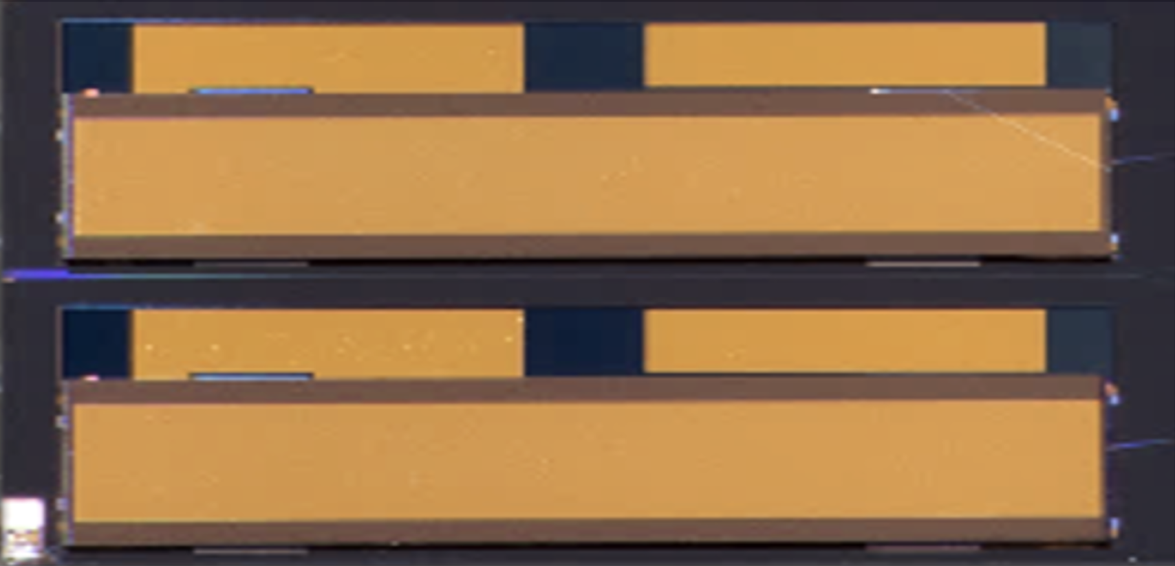
Our integrated photonics platforms are fabricated on 200-mm wafers using our 90-nm toolset in our cleanroom that has ISO 9001:2015 Certification. Our electron-beam lithography capabilities enable sub-90-nm features as needed. Extensive compound semiconductor fabrication and packaging facilities allow for the fabrication and integration of III-V and other devices. Flexible combination of fabrication modules is available.
Silicon Nitride and Alumina Visible Light Platform
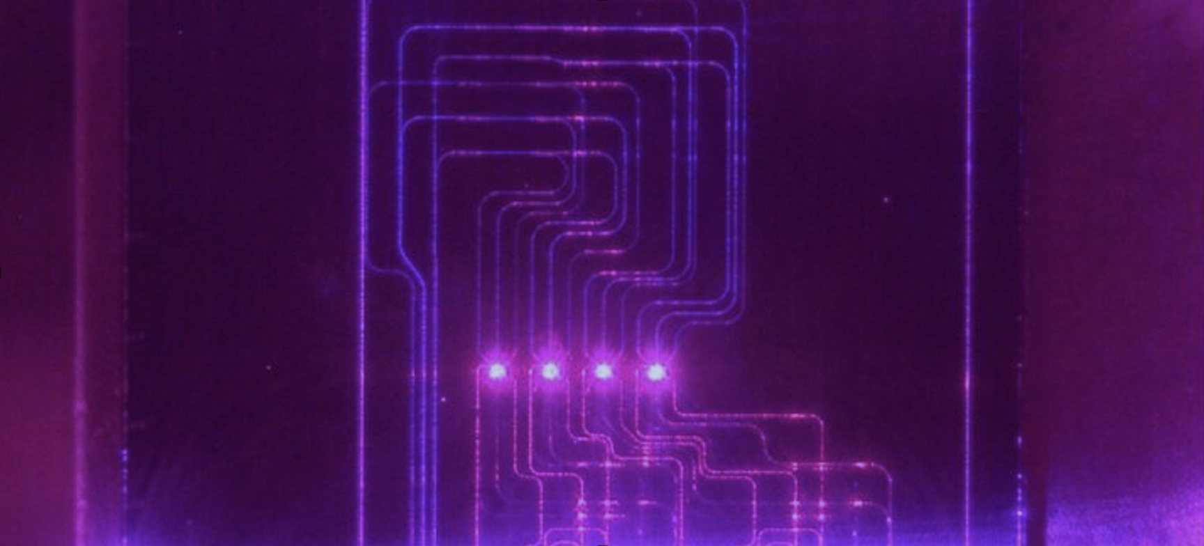
Our visible light platform is designed to cover optical wavelengths from 370–1092 nm. A mature passive component library provides fundamental devices at > 15 wavelengths throughout this band. Silicon nitride waveguide losses are < 0.3 dB/cm from the yellow to near infrared and < 0.1 dB/cm at 1100 nm. Alumina losses are in the 1–3 dB/cm range for the near-ultraviolet to the green. This platform supports multiple metal layers, including a ground plane under the photonics layers, and can be combined with silicon-based detectors and thermal heaters.
Silicon Nitride RF Photonic Platform
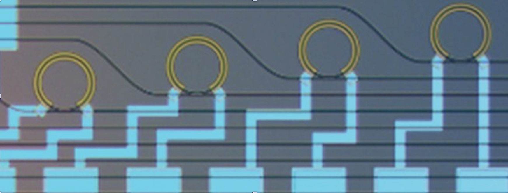
Our RF photonic platform is aimed at the telecom bands and optimized for RF, lidar, and sensing applications. Waveguide propagation losses are in the 0.1–0.2 dB/cm range, and an extensive component library includes reconfigurable filters, mode-division (de)multiplexers, and splitters among other components. We have demonstrated > 400 mW of optical power handling (measurement limited) and 10 kHz thermal tuning. Flip-chip integrated III-V lasers have shown in-waveguide powers up to 300 mW. Heterogenous integration of lithium niobate and III-V devices is in development.
Other Platforms

Our ultralow-loss, low-confinement silicon nitride platform has a loss of 0.5 dB/m, allows for long delays, and has been used along with dual-polarization temperature stabilization to yield a 20-Hz linewidth long-term SBS laser. We are also developing a germanium-based platform for the midwave infrared and have shown losses on the order of 1 dB/cm and GHz-class filters. We maintain a standard silicon photonics process and component library. Custom fabrication platforms may be available upon request.