Avalanche photodetector array integrated on readout integrated circuit.
Lincoln Laboratory offers a broad range of packaging capabilities for electrical systems, optical systems, and microsystems. Many of our capabilities are mature, established processes for delivering prototyped systems. We also conduct robust research and development to support next-generation systems.
Key Features
Electrical, optical, and microsystem packaging
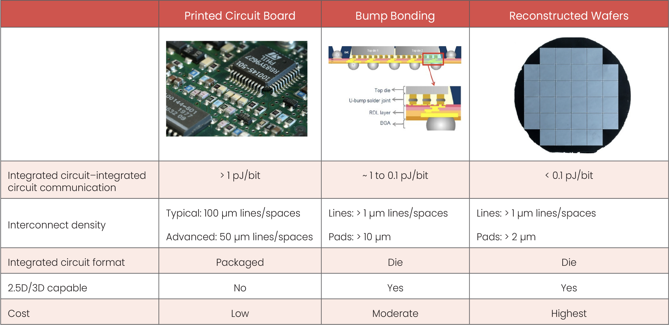
Electrical packaging including advanced printed circuit boards (PCBs), flip-chip bump bonding, 3D packages, and reconstructed wafers
Optical packaging including fiber fabrication; optical grinding, polishing, and coating; and photonic integrated circuits with heterogenous active components
Wafer-scale packaging and microsystems in fibers and fabrics
Electrical Packaging
Optical Fabrication and Packaging
A packaged high-power optical phased array.
Optical fibers
We can create custom optical fiber preforms, draw fibers, perform custom cleaving, splice optical fibers and interface them with external components, and overall conduct research and prototype optical fiber systems.
Optical components
Our optical fabrication facility enables precision optical assemblies, optical machining and polishing, and fused silica, silicon, optical glass, YAG, sapphire, YLF, and alumina component fabrication. In the optical coating facility, we can create custom high-fidelity optical coatings ranging from the X-ray to the infrared; antireflection coatings; beam splitters; black/hot/cold mirrors; and more.
Photonic integrated circuits (PICS)
We fabricate PICs with heterogenous integration of active components.
We also fabricate silicon-nitride and aluminum-oxide PICs that have achieved state-of-the-art specifications: > 400 mW power handling, 0.1 dB/cm loss (150 MHz filter linewidth), 10 kHz thermal tuning. In the area of hybrid photonic integration, we can integrate high-power lasers on chip. Our 300 mW on-chip optical power is a record level for a hybrid integrated laser.
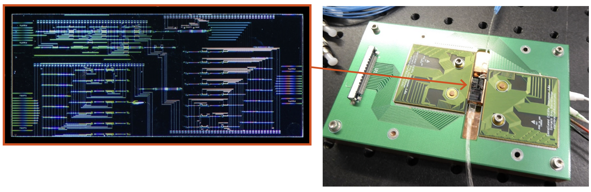
At left is an image of SiNx/SiO2-on-Si PIC, and at right, the PIC is integrated on a printed circuit interface board. The PIC was fabricated using the Laboratory's 200-mm silicon fabrication toolset, and contains approximately 80 components.
Microsystems Packaging
A wafer-scale multichip module
Wafer-scale packaging
Wafer-scale packaging leverages low-power communication and high interconnect density to create domain-specific accelerators. We integrate GPUs, FPGAs, and ASIC accelerators for compute-intense applications. Integrating memory close to the processor reduces latency and energy cost while increasing bandwidth. Wafer-scale multichip modules (MCMs) that integrate 2D and 3D stack-up together provide optimized solutions to meet the growing demands of artificial intelligence.
Functional fibers and fabrics
We functionalize fibers and fabrics through the incorporation of passive and active elements in the fibers. Microsystems integrated into fibers can be woven into soldier uniforms to improve physiological monitoring or be used to provide persistent monitoring of the undersea environment, among many applications.
For more information on Lincoln Laboratory's packaging capabilities, see this presentation.


 A packaged high-power optical phased array.
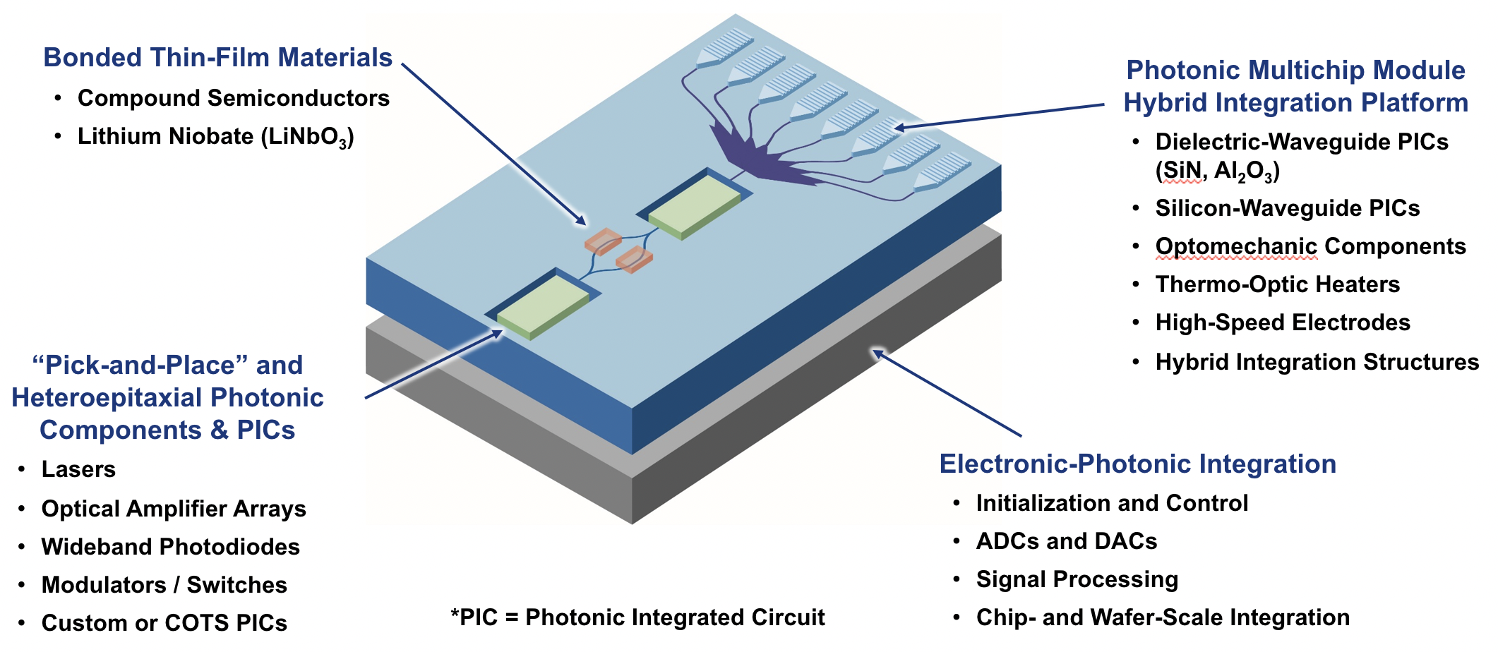
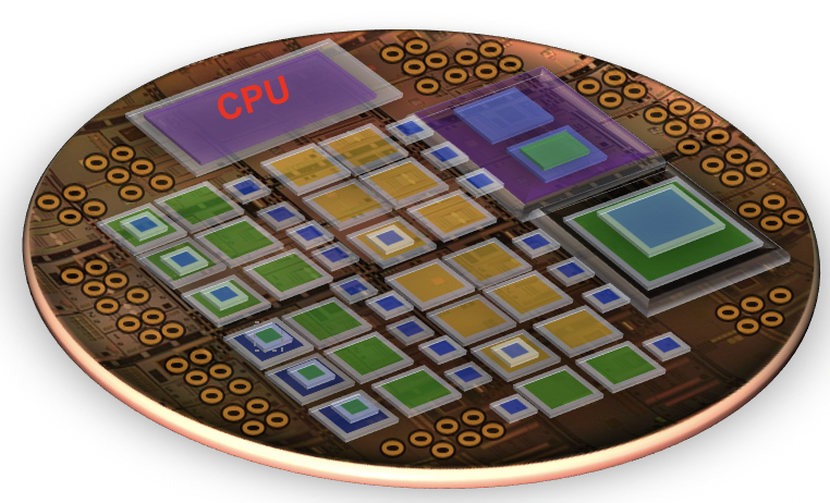 A wafer-scale multichip module