
- III-P/As/Sb epitaxy for optoelectronics heterostructures
- Close-coupled showerhead geometry
- Top-side pyrometric temperature control
- In situ reflectance and wafer curvature measurement
- Flexible wafer configurations from 7 x 2 in to 1 x 200 mm
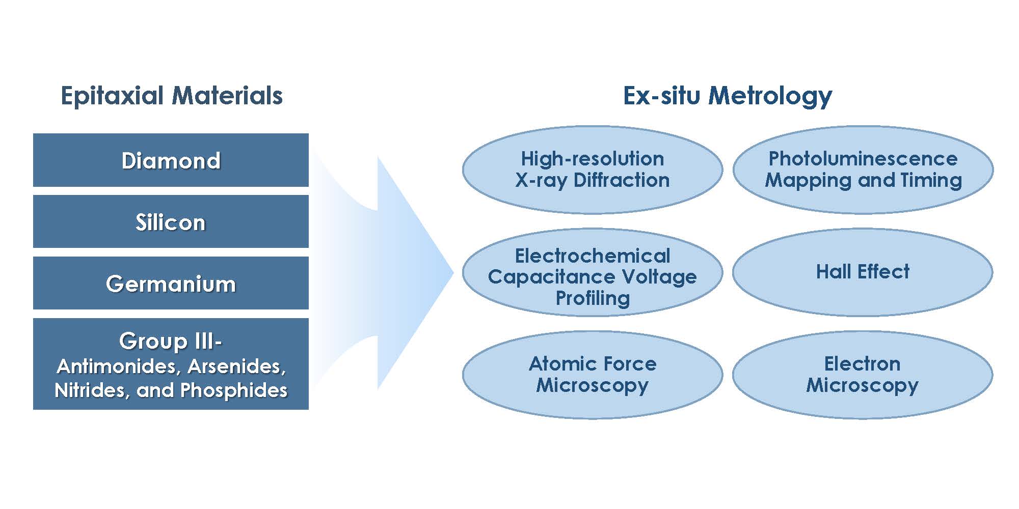
Materials
The Microsystems Prototyping Foundry has broad material systems capabilities for technology development in the electric, photonic, and quantum domains.
Compound Semiconductor Epitaxy

Aixtron CCS R&D Metal-Organic Chemical Vapor Deposition (MOCVD) Reactor

Dual Veeco MOD GEN II Molecular Beam Epitaxy (MBE) Reactors
- III-/As/Sb/Bi epitaxy for optoelectronic heterostructures
- Temperature monitoring via
- Band-edge thermometry
- Variable wavelength pyrometry
- Black body emission
- In situ reflection high-energy electron diffraction (RHEED)
- Al, Ga, In, As, Sb, Bi, Si, Be, and GaTe effusion cell sources
Silicon and Germanium Epitaxy

ASM Epsilon MOCVD Epitaxy
- 200-mm cassette to cassette
- Group 4 growth with P & N doping
- Si epitaxy for novel FET geometries
- Ge epitaxy on Si substrates
- SiGe epitaxy

Veeco GEN200 Molecular Beam Epitaxy
- Growth:
- 2 e-beam sources
- 5 effusion thermal sources
- 8 elements and counting: Al, B, Mo, Nb, Re, Sb, Si, Ta
- Analysis:
- Beam flux monitor
- Reflection high-energy electron diffraction (RHEED)
- Electron impact mission spectroscopy
- X-ray photoelectron spectroscopy
Contact us
Learn more about the capabilities and opportunities in the Microsystems Prototyping Foundry.