
Fully Depleted Silicon-on-Insulator CMOS

Lincoln Laboratory has a rich history of pioneering work on fully depleted silicon-on-insulator (FDSOI) CMOS thanks to a unique semiconductor research and fabrication facility with a modern 200-mm wafer tool set. We are the U.S. government microelectronics community’s only source of FDSOI technology in a facility that has ISO 9001:2015 Certification and is accredited for Trusted Design and Trusted Circuit Fabrication by the Defense Microelectronics Activity.
KEY FEATURES
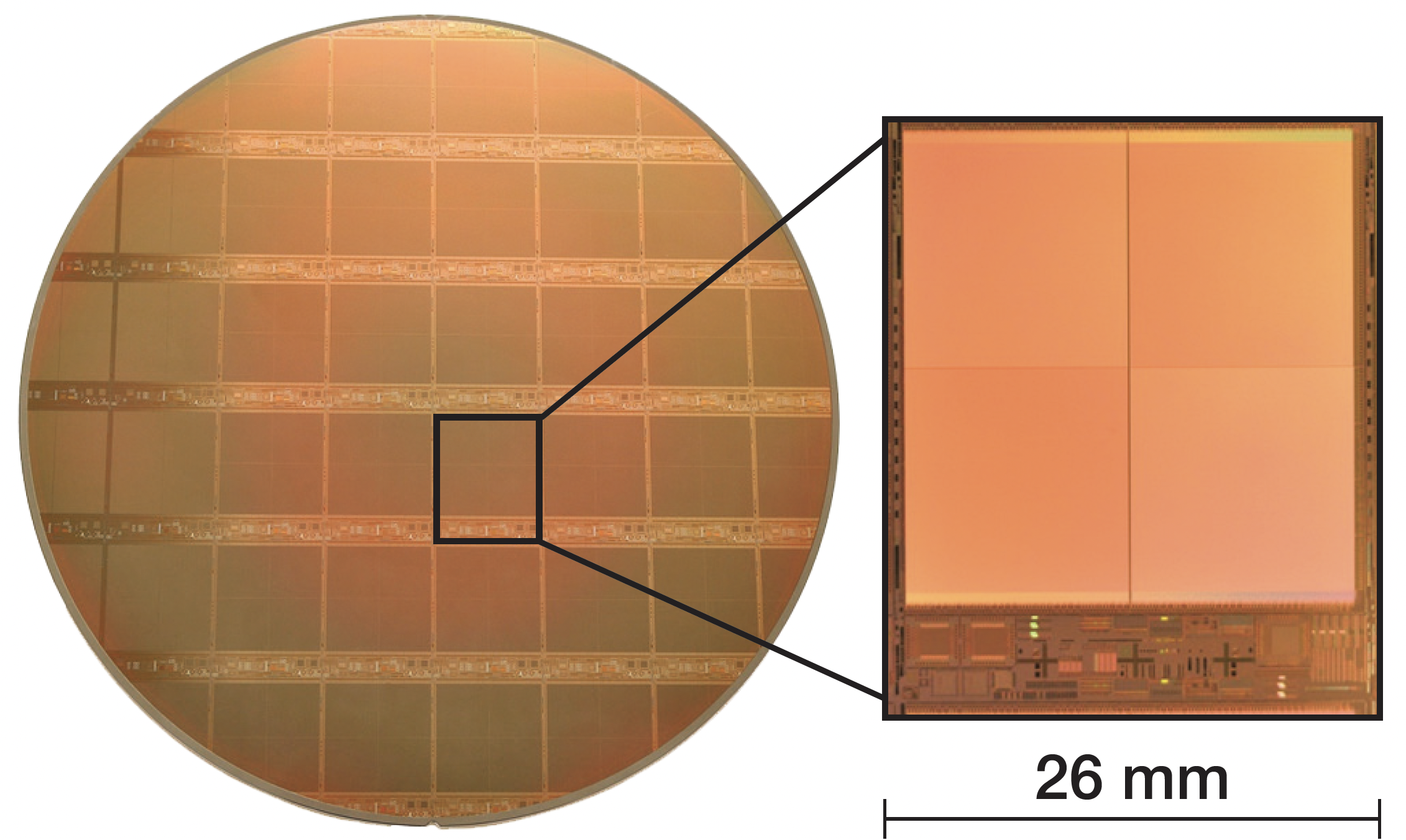
- 90-nm FDSOI CMOS on 200-mm-diameter wafers
- Specialized process variants optimized for very-low-power subthreshold operation, high-performance mixed-signal and RF applications, and extreme environment (cryogenic, high-temperature, and radiation) operation
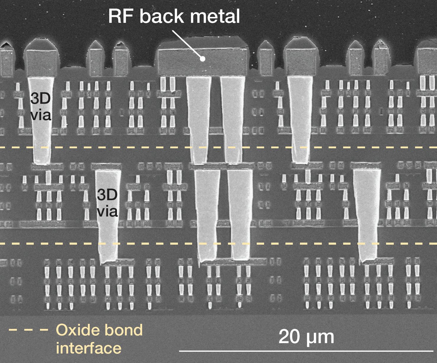
- Enabler for 2.5D and 3D heterogeneously integrated microsystems
Our facility supports a number of specialized CMOS processes at the 90-nm node:
- Extremely low-power technology for energy-starved systems
- Low-power readout circuits for very large focal plane arrays
- Power/speed optimized technology for cryogenic applications
- Thick-metal variant for high-performance mixed signal and RF systems
- Radiation-hardened variant for harsh environment applications
- High-temperature variant optimized for operation above 250°C
FDSOI CMOS Process Variants
-
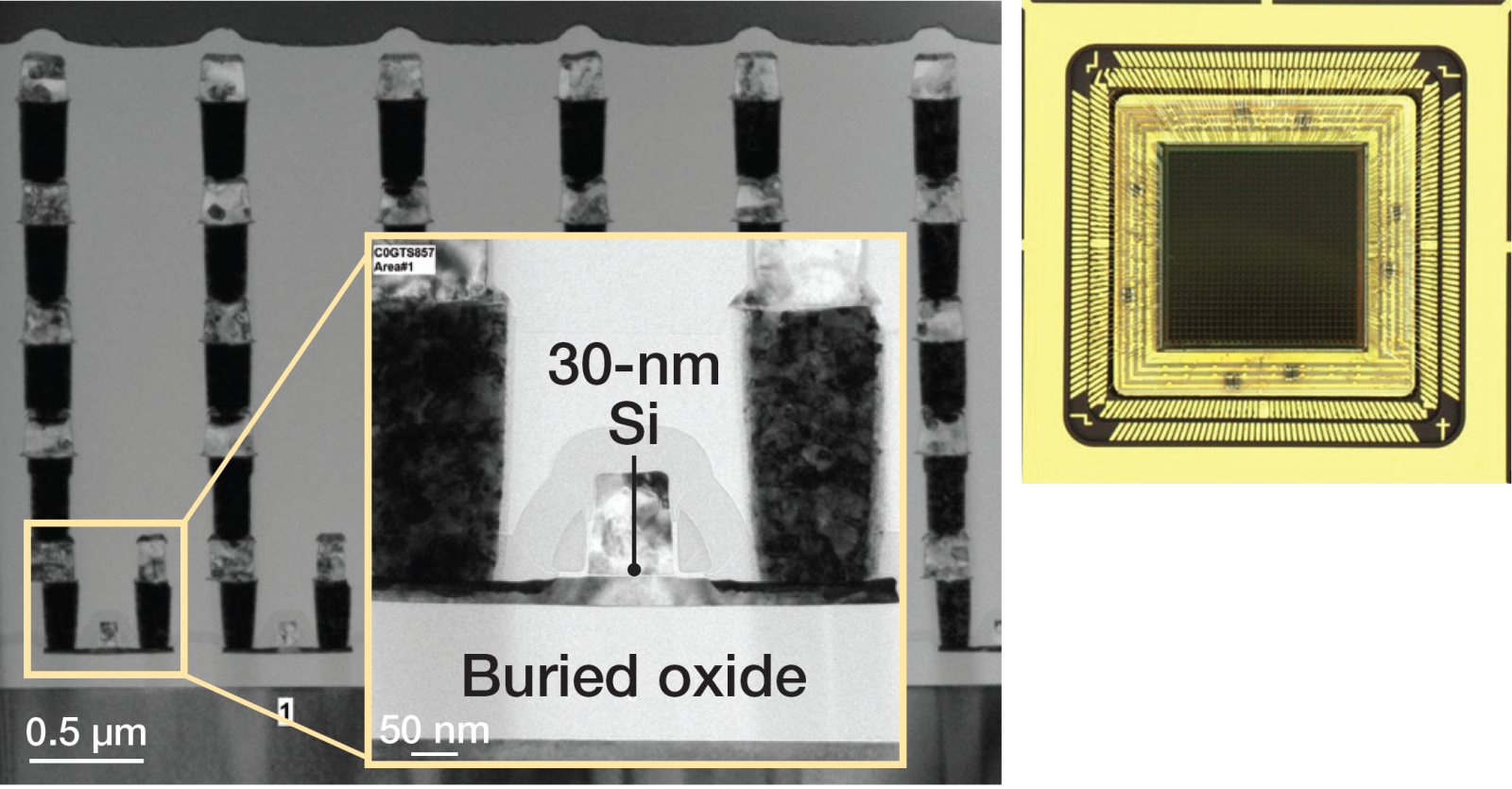
(090SOI12) is the baseline CMOS process, a 90-nm FDSOI poly-gate process with an ultra-shallow trench isolation, both low-and mid-threshold-voltage transistors designed for use in digital and analog applications at an operating voltage of 1.2 V. This five-level metal technology is available in standard and radiation-hardened versions. Two additional thick-metal levels are supported for mixed signal and RF applications. All fabrication steps in the front end and back end of line are supported onsite.
-
(200HVL25) is a higher-voltage variant of the 090SOI12 process that utilizes thicker 5.5-nm gate oxide with 200-nm poly gates for low-leakage operation. Dual-threshold 1.2-V and split-gate 2.5-V devices are available.
-
(090XLP03) is an extremely low-power transistor technology based on metal-gate FDSOI devices. These transistors are optimized for operation at 0.3 V and can realize a reduction in switching energy of 90% compared to conventional off-the-shelf 1.2-V bulk silicon.
-
(090CRYO04) is a variant of the baseline process that has been optimized for power and speed at cryogenic temperatures.
-
(045SOI) 45-nm node variant is under development
Design and Post-Fabrication Support
- Process Design Kit with a comprehensive design guide and technology model files to support custom circuit design in the baseline process and all variants
- Intellectual property design modules, Standard Cell and I/O libraries validated for Cadence simulation, synthesis and place and route tools
- Onsite reticle assembly, design-to-mask layer generation, and validation
- Onsite wafer dicing, advanced packaging, and electrical test capabilities