
Gallium Nitride on Silicon
Lincoln Laboratory developed fully silicon (Si) CMOS–compatible technologies for gallium nitride (GaN) monolithic microwave integrated circuits (MMICs) on 200-mm-diameter Si wafers. Measured fT and fmax are in the 50 and 90 GHz range, respectively, for GaN high-electron-mobility transistors (HEMTs) with 120-nm gate length on Si substrates. We are applying wafer-scale 3D integration technology to the heterogeneous integration of GaN MMICs and Si CMOS circuits for high-performance RF modules.
Key Features
-
CMOS-compatible process for GaN-on-Si MMICs
-
Use of 200-mm-diameter Si substrate and CMOS tools reduces cost and increases yield
-
Wafer-scale 3D integration of GaN MMICs with CMOS to enhance functionalities with improved size, weight, and power benefits
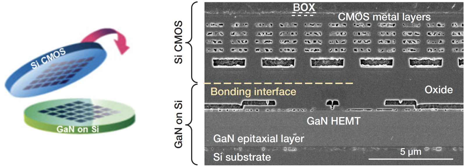
The 200-mm-diameter GaN-on-Si MMIC and Si CMOS wafers (above, left) are 3D integrated at the wafer scale. The two wafers are bonded face-to-face using a low-temperature oxide-oxide bonding technique. The Si substrate of the silicon-on-insulator wafer is completely removed by grinding and selective wet etch to stop at the buried oxide (BOX). Vias to the back of CMOS and to the top of GaN circuits are etched separately and interconnected with a top metal. The vertical integration minimizes the chip size and reduces the interconnect distance to lower the loss and delay. In addition to the oxide-oxide bond approach, work is underway to expand the capabilities of the 3D integration approach by using hybrid bond interconnects, which would allow direct electrical connections between the two wafers without separate vias to the GaN and CMOS circuits.
Features of Lincoln Laboratory Process
-
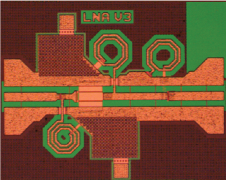 An X-band low-noise amplifier that delivers 10 dB gain. The GaN-on-Si MMIC process adds metal-insulator-metal capacitors, metal resistors, inductors, and 2 levels of interconnect metals. Design is possible with coplanar waveguide and microstrip processes.
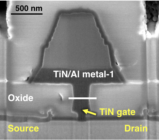
Growth of high-quality GaN HEMT layers on 200-mm-diameter Si substrates
-
Fully CMOS compatible with gold-free metallization
-
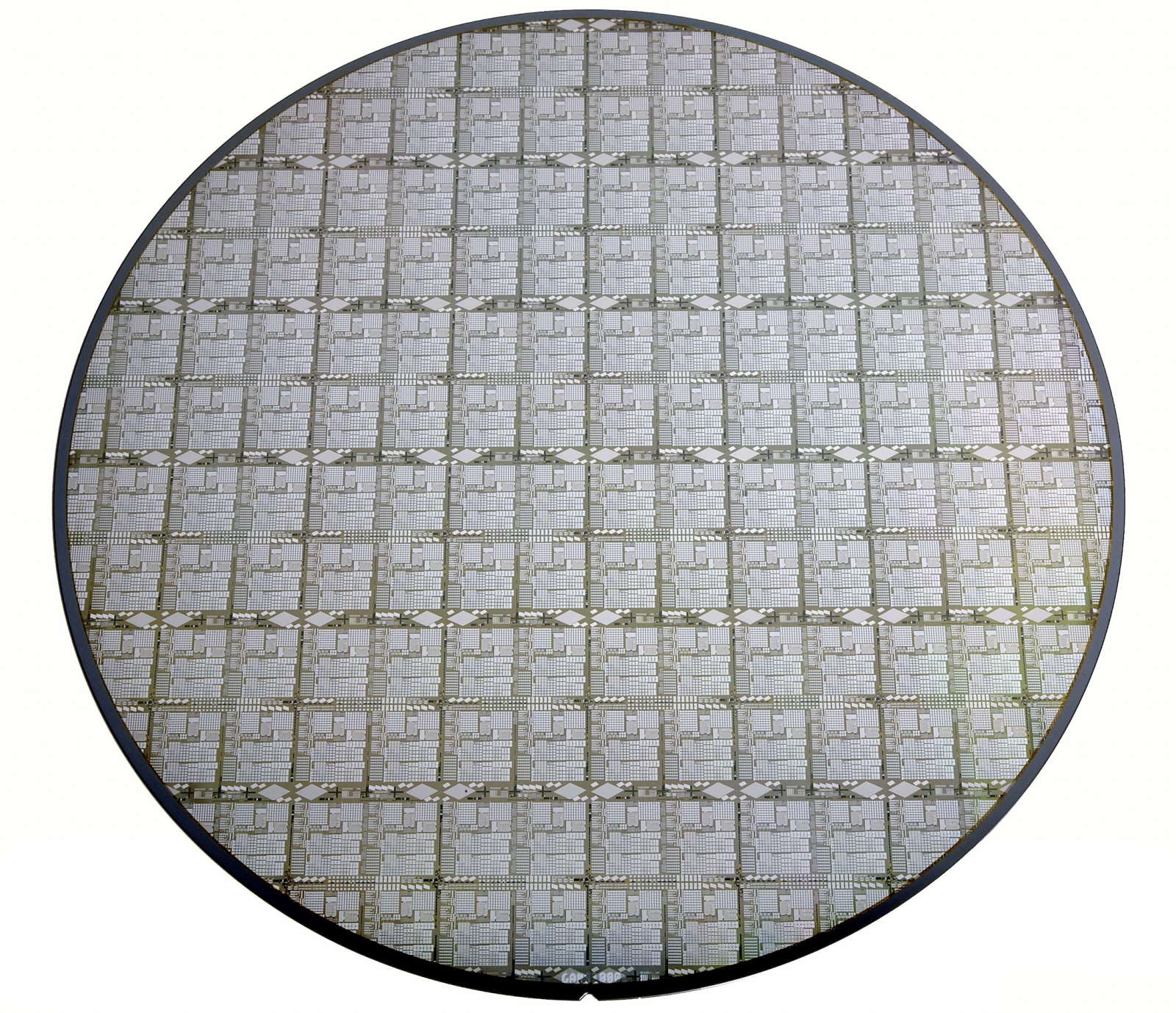
High yield and uniformity across 200-mm wafer
-
Breakdown voltage of approximately 90 V with 1-μm gate to drain spacing
-
Wafer-scale 3D integration with Si CMOS wafers, allowing multiple-tier wafer stacking
-
Integrated GaN-MMIC and CMOS circuits for high-performance RF modules with small size, weight, power, and cost
-
Use of standard CMOS processes and tools to enable direct technology transfer to Si foundries
Going Forward
-
The GaN-on-Si MMIC and Si CMOS 3D integration technology is available to external designs through multiple project wafer runs.
-
We provide models and process design kits for GaN MMICs and CMOS co-design and support.
-
Lincoln Laboratory facility has ISO 9001:2015 Certification and is accredited for Trusted design and aggregation through packaged circuit delivery.