
Superconducting Integrated Circuits
Lincoln Laboratory has developed the world's most advanced fabrication processes for superconductor integrated circuits. This research foundry capability enables prototyping of advanced single-flux-quantum (SFQ), quantum flux parametron (QFP), and other types of digital, mixed signal, analog, and neuromorphic circuits, along with flip-chip packaging on superconducting multichip modules.
Key Features
-
Superconductive SFQ circuits with ultrafast switching speed and low switching energy unmatched by any other demonstrated integrated circuit technology
-
Adiabatic quantum flux parametron circuits with ultralow energy dissipation down to the Landauer's thermodynamic limit
-
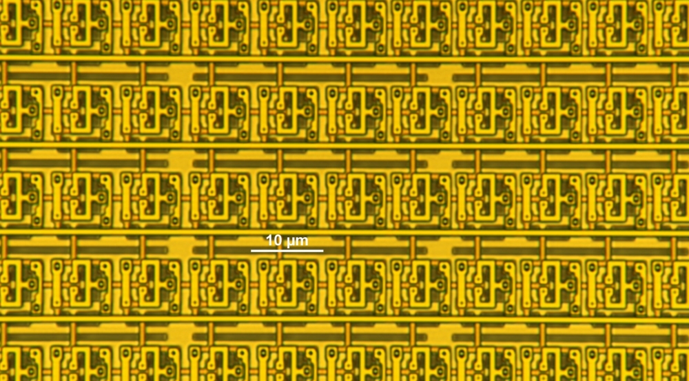
SFQ circuits demonstrated with up to 809,000 Josephson junctions, a world record
Lincoln Laboratory Processes
Multiple SFQ research foundry fabrication process nodes are either offered or under development, as outlined in the Lincoln Laboratory SFQ Technology Roadmap. The table below outlines key features and dimensions offered for each process node. By adding more superconducting layers for circuit inductors and data routing, and reducing minimum linewidth and size of vias, circuit densities exceeding 2x10⁷ Josephson junctions per cm2 can be achieved. New process features are first made available to circuit design teams while the process is matured.
A new high-Jc process, SFQ5hs, is available from 2017. Future nodes, such as SFQ7ee, feature additional layers of high kinetic inductance materials and reduced minimum feature sizes.
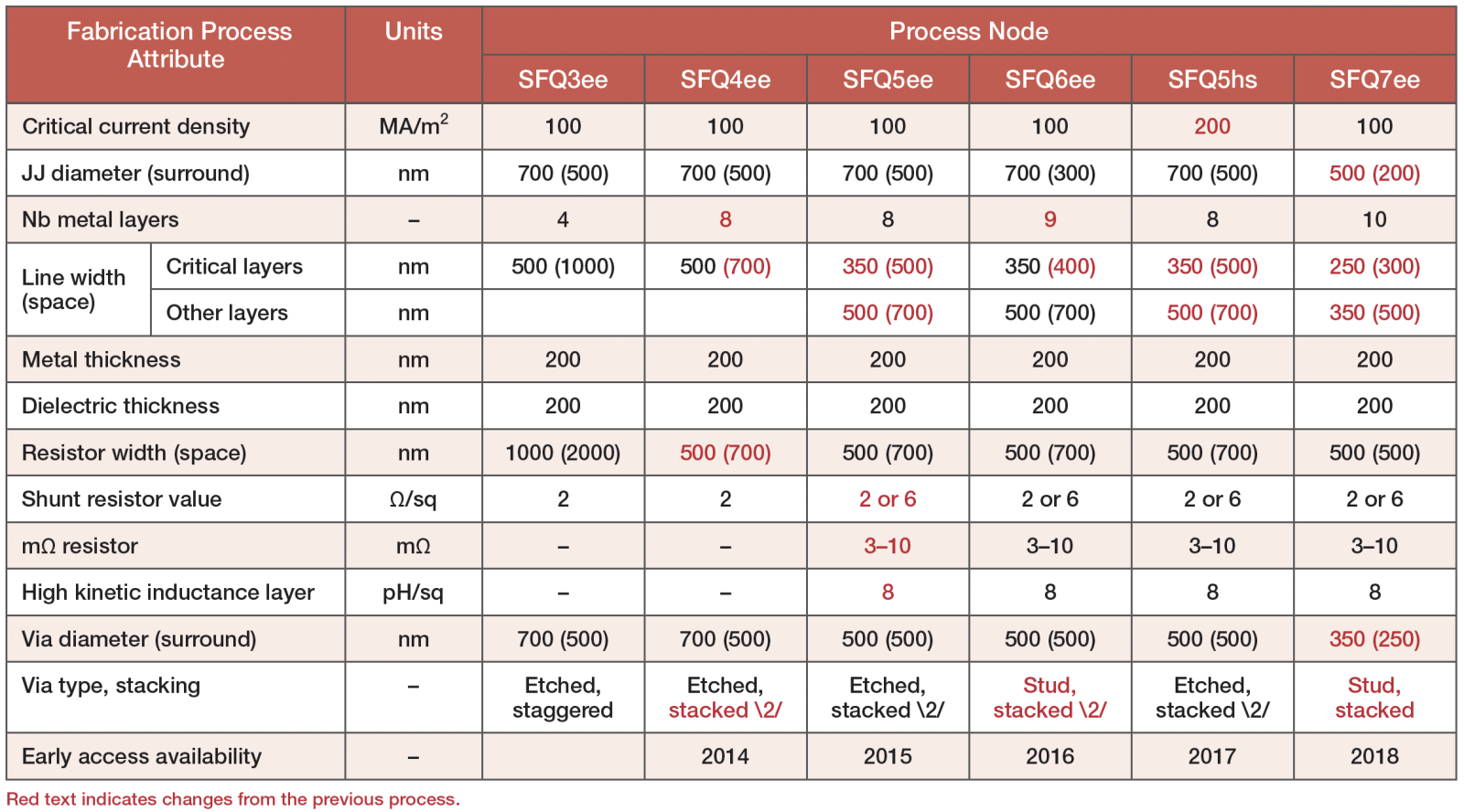
SFQ5ee Process Node
The SFQ5ee process provides attractive features:
- 700-nm Josephson junctions
- Eight niobium wiring layers
- 350-nm wiring feature size
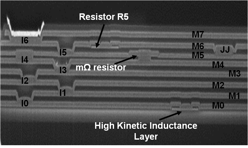
- High-kinetic-inductance layer
Applications
Our SFQ integrated circuits can have application in a variety of fields:
- High-performance digital computing
- Wideband mixed RF/digital processing
- Quantum computing
Contact