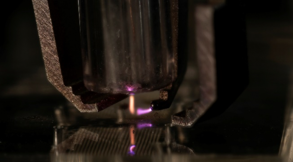
Microplasma Sputterer
3D printing has revolutionized manufacturing, allowing tiny mechanical parts that were impossible to machine conventionally to be built through a process of depositing successive layers of materials, like a plastic or metal. Yet, 3D printing electronic systems along with these mechanical parts remains a challenge. The only current way to manufacture the conductive lines (called interconnects) that connect microelectronic components is by using photolithography and etching processes in a cleanroom.
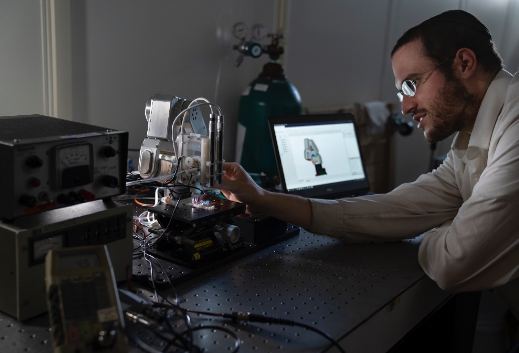
With MIT collaborators, we've developed a new method for manufacturing interconnects. Our system uses plasma to "sputter" atoms in a jet that forms metal lines directly on a substrate. Unlike traditional sputtering techniques that are conducted in vacuum chambers to reduce scattering, our process uses electrostatic fields to focus the beam of sputtered atoms to a very narrow region, enabling us to directly write interconnect on nonplanar surfaces. Using our prototype microsputtering print head, which is being designed to work with existing 3D-printing systems, we’ve deposited conductive gold lines ranging in width from 1 um to 100 um on a range of substrates, including silicon, glass, and polymers. These interconnects have electrical properties comparable to those produced using standard photolithography and etching processes.
Our long-term goal is to expand microplasma sputtering capabilities to print a range of high-performance electrical, optical, and magnetic materials and to integrate them with our direct ink write technologies. We believe the ability to print complete electronic systems along with structural components in the same 3D-printing environment can revolutionize microsystems manufacturing.
Related
News


Massachusetts wins proposal to host Northeast Microelectronics Hub through Federal CHIPS and Science Act

MIT engineers “grow” atomically thin transistors on top of computer chips
Publications
Seismic barrier protection of critical infrastructure
Effect of surface roughness and H-termination chemistry on diamond's semiconducting surface conductance
Large enhancement of third-order nonlinear effects with a resonant all-dielectric metasurface
Comparison of gate dielectric plasma damage from plasma-enhanced atomic layer deposited and magnetron sputtered TiN metal gates
Staff